Gate finger gradually-widened GaN FinFET structure and preparation method thereof

A gate finger and heterostructure technology, which is applied in the field of GaNFinFET structure with gradually widened gate fingers and its preparation, can solve the problems that the FinFET structure is difficult to take into account the withstand voltage and frequency of the device, and it is difficult to realize high-power high-frequency devices, etc., to achieve relief Effects of current collapse, mitigation of scattering, and improvement of withstand voltage performance

Active Publication Date: 2020-06-02
浙江集迈科微电子有限公司
View PDF4 Cites 2 Cited by
  • Summary
  • Abstract
  • Description
  • Claims
  • Application Information

AI Technical Summary

Problems solved by technology

[0004] In view of the above-mentioned shortcomings of the prior art, the object of the present invention is to provide a GaNFinFET structure with gradually widening gate fingers and its preparation method, which is used

Method used


Image

  • Gate finger gradually-widened GaN FinFET structure and preparation method thereof
  • Gate finger gradually-widened GaN FinFET structure and preparation method thereof
  • Gate finger gradually-widened GaN FinFET structure and preparation method thereof

Examples


Embodiment 1

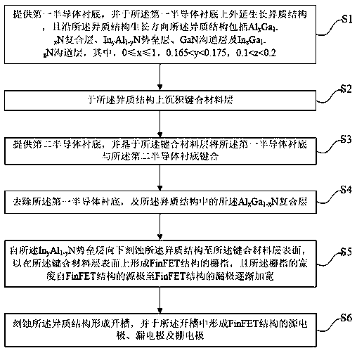
[0046] This embodiment provides a method for fabricating a GaN FinFET structure with gradually wider gate fingers, using a GaN / InGaN double channel instead of a traditional GaN single channel. On the one hand, the effective mass of carriers in the InGaN channel is lower than that of the GaN channel. The effective mass of the carrier can effectively improve the drift velocity of the upper limit carrier in the FinFET structure, and realize the high frequency response of the FinFET structure. At the same time, the relatively narrow band gap of the InGaN material can make the two-dimensional electron gas (2DEG) better Confined in the channel, effectively alleviate carrier scattering and current collapse; in addition, the gate fingers in the FinFET structure are designed to gradually widen from the source to the drain direction, effectively improving the withstand voltage performance of the FinFET structure.

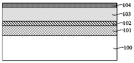
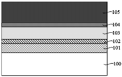
[0047] Such as Figure 1 to Figure 12 Shown, described preparation metho...

Embodiment 2

[0075] This embodiment provides a GaN FinFET structure with gradually wider gate fingers. The FinFET structure can be prepared by the preparation method of the first embodiment above, but is not limited to the preparation method described in the first embodiment, as long as the structure can be formed. For the beneficial effects achieved by the FinFET structure, please refer to Embodiment 1, which will not be described in detail below.

[0076] Such as Figure 6 to Figure 9 As shown, the FinFET structure includes:

[0077] a second semiconductor substrate 106;

[0078] a bonding material layer 105 located on the second semiconductor substrate 106;

[0079] The FinFET structure is located on the bonding material layer 105, and the FinFET structure includes: a gate 113, a source 108, a drain 109 and a gate finger 107, wherein the source 108, the drain 109 and the gate finger 107 are composed of Cascading In y al 1-y N barrier layer 102, GaN channel layer 103 and In z Ga 1...


PUM

PropertyMeasurementUnit
Thicknessaaaaaaaaaa
Thicknessaaaaaaaaaa
Thicknessaaaaaaaaaa

Abstract

The invention provides a gate finger gradually-widened GaN FinFET structure and a preparation method thereof. The structure comprises a second semiconductor substrate, a bonding material layer locatedon the second semiconductor substrate, and a FinFET structure located on the bonding material layer, wherein the FinFET structure comprises a grid electrode, a source electrode, a drain electrode anda gate finger, the source electrode, the drain electrode and the gate finger are formed by an InyAl<1-y>N barrier layer, a GaN channel layer and an InzGa<1-z>N channel layer which are stacked in sequence, y is greater than 0.165 and less than 0.175, z is greater than 0.1 and less than 0.2, the two ends of the gate finger are connected with the source electrode and the drain electrode respectively, and the width of the gate finger is gradually increased from the source electrode to the drain electrode. GaN/InGaN double channels are adopted; on the one hand, the effective mass of carriers in the InGaN channel is lower than that of carriers in the GaN channel, so that the drift speed of upper limit carriers in the FinFET structure is effectively improved; meanwhile, two-dimensional electrongas (2DEG) can be better limited in the channel through a relatively narrow band gap of the InGaN material, and scattering and current collapse of the carriers are effectively relieved; in addition, the gate finger in the FinFET structure is designed to be in a gradually widened shape, so that the voltage withstanding performance of the FinFET structure is effectively improved.

Description

technical field [0001] The invention belongs to the field of semiconductor manufacturing, in particular to a GaN FinFET structure with gradually widened gate fingers and a preparation method thereof. Background technique [0002] As we all know, power electronic systems have always contributed to sustainable development and improved energy conversion rates. As one of the key components of energy conversion in power electronic systems, power semiconductor devices have always been the research focus of many scholars. As a representative of the third-generation semiconductor materials, GaN has a large band gap, high carrier mobility, and high breakdown voltage, and has been identified as a significant candidate for high-voltage, high-power, and high-frequency applications candidate. GaN-based semiconductor devices commonly used in the industry include GaN HEMT devices, GaN FinFETs and nanowire structures. [0003] Existing GaN HEMT devices usually have a planar structure, th...

Claims


Application Information

Patent Timeline
IPC IPC(8): H01L29/778H01L29/423H01L21/335
CPCH01L29/42316H01L29/66462H01L29/7783
Inventor 马飞冯光建蔡永清
Owner 浙江集迈科微电子有限公司
Why Eureka
Try Eureka