Trench MOSFET and manufacturing method thereof

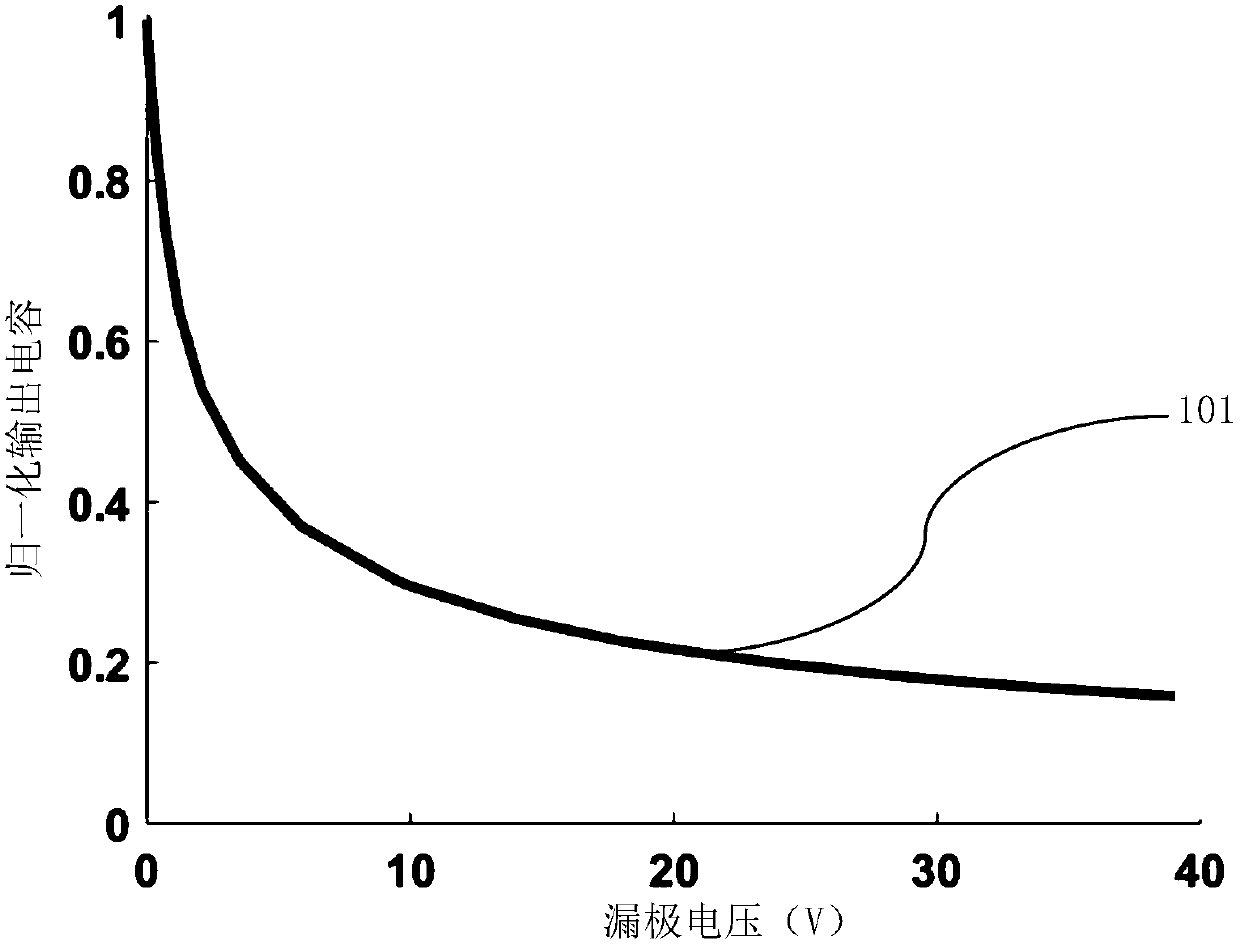
A manufacturing method and trench technology, applied in semiconductor/solid-state device manufacturing, electrical components, circuits, etc., can solve problems such as input capacitance drop

Pending Publication Date: 2020-06-02
SHENZHEN SANRISE TECH CO LTD
View PDF7 Cites 1 Cited by
  • Summary
  • Abstract
  • Description
  • Claims
  • Application Information

AI Technical Summary

Problems solved by technology

like figure 2 Shown is the output capacitance curve of the existing trench MOSFET; where curve 101 is the output capacitance curve of the existing trench MOSFET, the abscissa of the output capacitance curve is the drain voltage, the ordinate is the normalized capacitance, and the normalized Capacitor 1 ha

Method used


Image

  • Trench MOSFET and manufacturing method thereof
  • Trench MOSFET and manufacturing method thereof
  • Trench MOSFET and manufacturing method thereof

Examples


no. 1 example

[0077] Trench MOSFET according to the first embodiment of the present invention:

[0078] The trench MOSFET according to the first embodiment of the present invention includes: a primitive cell region and a peripheral region, and the peripheral region is located on the periphery of the primitive cell region.

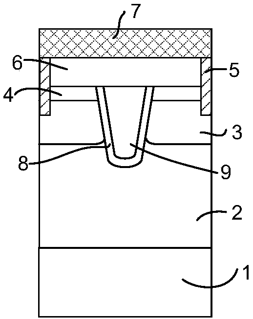
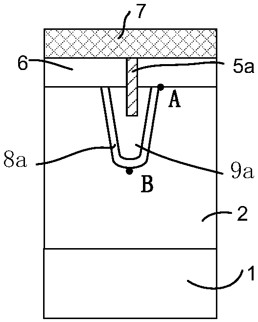
[0079] The device unit structure of the trench MOSFET is formed in the original cell area, and the device unit structure of each device please refer to figure 1 As shown, each of the device unit structures includes:

[0080] The first trench gate is formed by stacking the first gate dielectric layer 8 and the first polysilicon gate 9 formed in the first trench.

[0081] The drift region 2 is composed of the first epitaxial layer 2 doped with the first conductivity type.

[0082] The body region 3 is composed of a doped region of the second conductivity type formed on the surface of the drift region 2 .

[0083] The source region 4 is composed of a heavily doped region...


PUM


Abstract

The invention discloses a trench metal oxide semiconductor field effect transistor (MOSFET). The structure comprises a primitive cell region and a peripheral region, wherein a device unit structure ofa trench MOSFET is formed in the primitive cell region, a trench MOS capacitor used for reducing the nonlinearity of the output capacitance of the trench MOSFET is formed in the peripheral region, and the trench MOS capacitor comprises a second trench gate formed by superposing a second gate dielectric layer and a second polysilicon gate which are formed in a second trench; a source region is notformed on the surface of the first epitaxial layer covered on the side surface of the second polysilicon gate, a drift region formed by the first epitaxial layer extends into the whole primitive cellregion and the peripheral region, and a drain region is formed on the back surface of the drift region; the top of the second polysilicon gate is connected to the source electrode through a contact hole; the trench MOS capacitor and the device unit structure form a parallel structure, and the output capacitance of the whole trench MOSFET is improved and the nonlinearity of the output capacitanceis reduced when the device is reversely biased. The invention further discloses a manufacturing method of the trench MOSFET.

Description

technical field [0001] The invention relates to the field of manufacturing semiconductor integrated circuits, in particular to a trench MOSFET; the invention also relates to a method for manufacturing the trench MOSFET. Background technique [0002] Such as figure 1 As shown, it is a structural schematic diagram of the device unit structure of the existing trench MOSFET. The existing trench MOSFET is formed by connecting multiple device unit structures in parallel. Each of the device unit structures includes: [0003] The first trench gate is formed by stacking the first gate dielectric layer 8 and the first polysilicon gate 9 formed in the first trench. [0004] The drift region 2 is composed of the first epitaxial layer 2 doped with the first conductivity type. [0005] The body region 3 is composed of a doped region of the second conductivity type formed on the surface of the drift region 2 . [0006] The source region 4 is composed of a heavily doped region of the fir...

Claims


Application Information

Patent Timeline
IPC IPC(8): H01L29/78H01L29/423H01L21/336
CPCH01L29/7813H01L29/66734H01L29/4236Y02B70/10
Inventor 蒋容肖胜安
Owner SHENZHEN SANRISE TECH CO LTD
Why Eureka
Try Eureka