

Method and device for depositing thin film on inner wall of small hole
A technology of film deposition and hole inner wall, applied in metal material coating process, vacuum evaporation coating, coating and other directions, can solve the problems of cost production efficiency limitation, high target ion density, high sputtering power, etc. Large-scale low-cost production, improved deposition efficiency, and high universality
- Summary
- Abstract
- Description
- Claims
- Application Information
AI Technical Summary
Problems solved by technology
Method used
Image

Examples
Embodiment 1
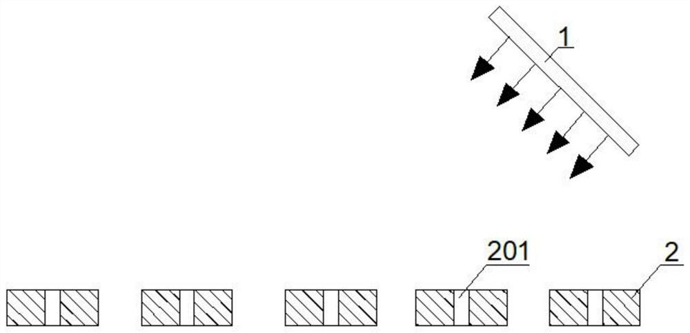
[0037] A thin film deposition method on the inner wall of a small hole, such as image 3 As shown, the target 1 is arranged obliquely above the material 2 to be sputtered, so that the target ions strike the inner wall of the small hole 201 of the material 2 to be sputtered at a set angle. In this embodiment, 95% alumina ceramics are used as the material 2 to be sputtered, and the material 2 to be sputtered is provided with a small hole 201 with a diameter of 0.2 mm and a depth of 1.2 mm, and a Ti metal thin film is formed on the inner wall of the small hole 201. deposition.
[0038] The deposition method of this embodiment specifically includes the following steps:
[0039] (1) Ultrasonic cleaning is performed on alumina ceramics for 10-20 minutes. After being dried with 99.9% dry nitrogen for 3 minutes, it is dried in an oven for 20-30 minutes under an air atmosphere at a drying temperature of 150-200° C. to obtain the Sputtering material 2: check the material 2 to be sputt...
Embodiment 2
[0043] In this embodiment, zirconia ceramics are used as the material 2 to be sputtered, and a small hole 201 with a diameter of 30 mm and a depth of 210 mm is opened on the material 2 to be sputtered, and Si film is deposited on the inner wall of the small hole 201 .
[0044] The deposition method of this embodiment specifically includes the following steps:
[0045] (1) Ultrasonic cleaning is performed on zirconia ceramics for 10-20 minutes, and after drying with 99.9% dry nitrogen for 3 minutes, they are dried in an oven for 20-30 minutes under an air atmosphere at a drying temperature of 150-200° C. Sputtering material 2: check the material 2 to be sputtered to ensure that the inner wall of the small hole 201 is clean and free of impurities, and perform radio frequency cleaning before magnetron sputtering. The power of the radio frequency cleaning is 100W, and the cleaning time is 3-5 minutes.
[0046] (2) Use target 1 (Si target) to start magnetron sputtering, the angle bet...
Embodiment 3
[0049] In this embodiment, Fe is used as the material 2 to be sputtered, and a small hole 201 with a diameter of 100 mm and a depth of 300 mm is opened on the material 2 to be sputtered, and a Mo metal thin film is deposited on the inner wall of the small hole 201 .
[0050] The deposition method of this embodiment specifically includes the following steps:
[0051] (1) Ultrasonic cleaning is performed on Fe for 10-20 minutes. After being blown dry with 99.9% dry nitrogen for 3 minutes, it is dried in an oven for 20-30 minutes under an air atmosphere at a drying temperature of 150-200° C. to obtain the Material 2: Check the material 2 to be sputtered to ensure that the inner wall of the small hole 201 is clean and free of impurities, and perform radio frequency cleaning before magnetron sputtering. The power of the radio frequency cleaning is 100W for 3-5 minutes.
[0052] (2) Use target 1 (Mo target) to start magnetron sputtering, the angle between target 1 and the vertical s...
PUM
| Property | Measurement | Unit |
|---|---|---|
| diameter | aaaaa | aaaaa |
| diameter | aaaaa | aaaaa |
| diameter | aaaaa | aaaaa |
Abstract
Description
Claims
Application Information