Ultra-wideband intermediate infrared band perfect wave absorber and preparation method thereof

An infrared band and ultra-broadband technology, applied in the field of mid-infrared perfect absorber and its preparation, can solve the problems of narrow absorption band, low efficiency, narrow absorption bandwidth, etc., and achieve the effect of low cost and high-efficiency absorbing response

Inactive Publication Date: 2020-06-05
JIANGXI NORMAL UNIV
View PDF6 Cites 11 Cited by
  • Summary
  • Abstract
  • Description
  • Claims
  • Application Information

AI Technical Summary

Problems solved by technology

However, there are still defects such as narrow absorption bandwidth, low efficiency, complex structure and the need to use precious metal materials.
Some existing broadband absorbers absorb only one resonance wavelength, and the absorption band is narrow

Method used


Image

  • Ultra-wideband intermediate infrared band perfect wave absorber and preparation method thereof
  • Ultra-wideband intermediate infrared band perfect wave absorber and preparation method thereof
  • Ultra-wideband intermediate infrared band perfect wave absorber and preparation method thereof

Examples


Embodiment 1

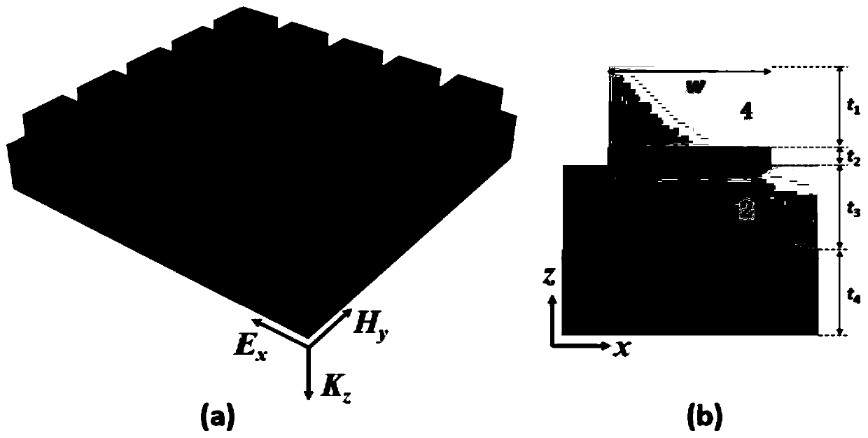
[0048] The ultra-broadband mid-infrared band perfect wave absorber in this embodiment adopts two kinds of materials, chromium and alumina. First, a layer of chromium with a thickness of 150 nanometers is sequentially deposited on the substrate silica glass sheet by physical vacuum coating method. film, a layer of aluminum oxide film with a thickness of 170 nm, a layer of chromium film with a thickness of 15 nm, and a layer of aluminum oxide film with a thickness of 180 nm; The dielectric / metal nanocubes are prepared by etching technology as a periodic periodic array, the array period (P) is 250 nanometers, the side length (W) of the nanocubes is 220 nanometers, and the thickness of the flat metal film (t 4) is 150 nm, and the flat dielectric film thickness (t 3 ) is 170 nm, the thickness of the metal nanocube (t 2 ) is 15 nm, and the thickness of the dielectric nanocube (t 1 ) is 180 nm. The surrounding environment is air.

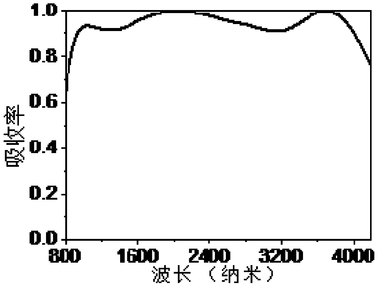
[0049] Such as figure 2 As shown, from the nea...

Embodiment 2

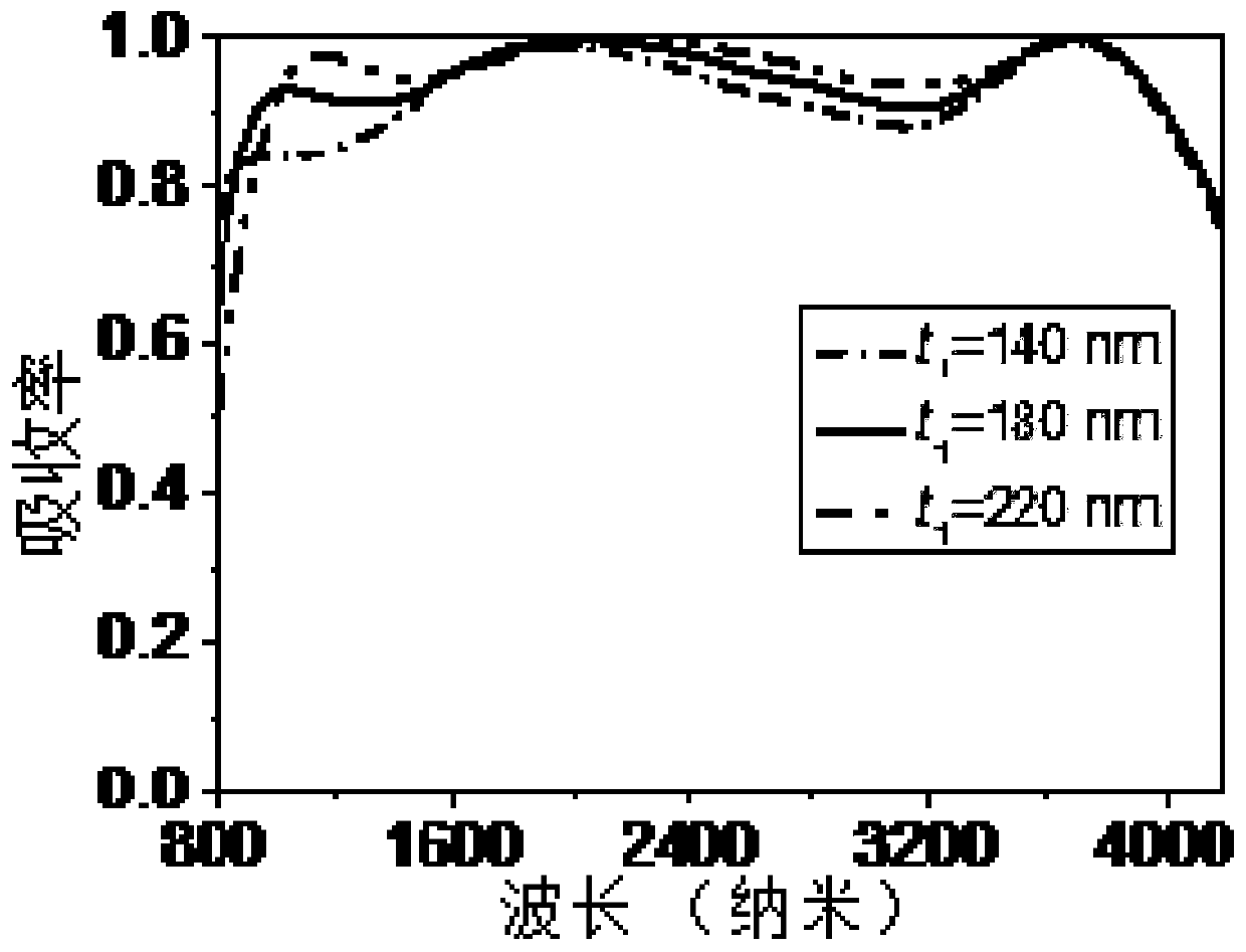
[0051] The top layer of the ultra-broadband mid-infrared band perfect wave absorber in this embodiment is a dielectric alumina nanocube with a thickness of 140 nanometers, and other parameters are the same as those in Embodiment 1. To test, you can get as image 3 The corresponding absorption spectra are shown.

Embodiment 3

[0053] The top layer of the ultra-broadband mid-infrared band perfect wave absorber in this embodiment is a dielectric alumina nanocube with a thickness of 180 nanometers, and other parameters are the same as those in Embodiment 1. To test, you can get as image 3 As shown in the corresponding absorption spectrum graph, the absorber should absorb more than 90% of the broadband up to 3059 nm, from 939 nm to 3998 nm.


PUM

PropertyMeasurementUnit
thicknessaaaaaaaaaa
thicknessaaaaaaaaaa
thicknessaaaaaaaaaa

Abstract

The invention provides an ultra-wideband intermediate infrared band perfect wave absorber and a preparation method thereof. The ultra-wideband intermediate infrared band perfect wave absorber is sequentially composed of a flat metal film layer, a flat dielectric film layer, a metal nanocube array and a dielectric nanocube array from bottom to top. The metal can be chromium, titanium, nickel, tungsten and the like, and the dielectric medium can be aluminum oxide, silicon dioxide, magnesium fluoride, zinc oxide and the like. The absorber is simple and mature in process preparation, can realize perfect absorption from a near-infrared band to a intermediate infrared band, and has the characteristics of wide absorption band, high absorption efficiency, insensitive angle and good thermal stability.

Description

technical field [0001] The invention relates to an optical element, in particular to a mid-infrared perfect absorber and a preparation method thereof. Background technique [0002] Since Landy et al. reported a perfect metamaterial absorber in 2008, perfect absorbers have attracted extensive attention and made great progress. Broadband perfect absorbers have promising applications, such as solar cells, thermal emitters, and imaging devices. [0003] Absorbers can be divided into single-band, dual-band, multi-band and broadband absorbers according to different types. The absorber mainly consists of a metal-dielectric-metal three-layer structure. The absorptivity can be expressed as A=1-R-T, where A represents the absorptivity, R represents the reflectivity, and T represents the transmittance. Since the bottom metal layer is to prevent electromagnetic transmission (that is, the transmittance is 0), and the top metal structure is to match the absorber impedance to suppress r...

Claims


Application Information

Patent Timeline
Patent Type & Authority Applications(China)
IPC IPC(8): G02B5/00G02B1/00
CPCG02B5/003G02B1/00
Inventor 吴彪周进刘桂强刘晓山刘忠民付国兰刘正奇
Owner JIANGXI NORMAL UNIV
Why Eureka
Try Eureka