Semiconductor device

A semiconductor and device technology, applied in the field of three-dimensional stacked semiconductor devices, can solve problems such as interference, unfavorable 3D integrated circuit integration and promotion, and achieve the effect of reducing production costs

Pending Publication Date: 2020-06-05
YANGTZE MEMORY TECH CO LTD
View PDF4 Cites 0 Cited by
  • Summary
  • Abstract
  • Description
  • Claims
  • Application Information

AI Technical Summary

Problems solved by technology

[0004] However, the above-mentioned 3D stacking technology still has many deficiencies, such as the interference between the external connection and the semiconductor device in the stacked chip, which is not conducive to the integration and improvement of the overall performance of the 3D integrated circuit.

Method used


Image

  • Semiconductor device
  • Semiconductor device
  • Semiconductor device

Examples


Embodiment Construction

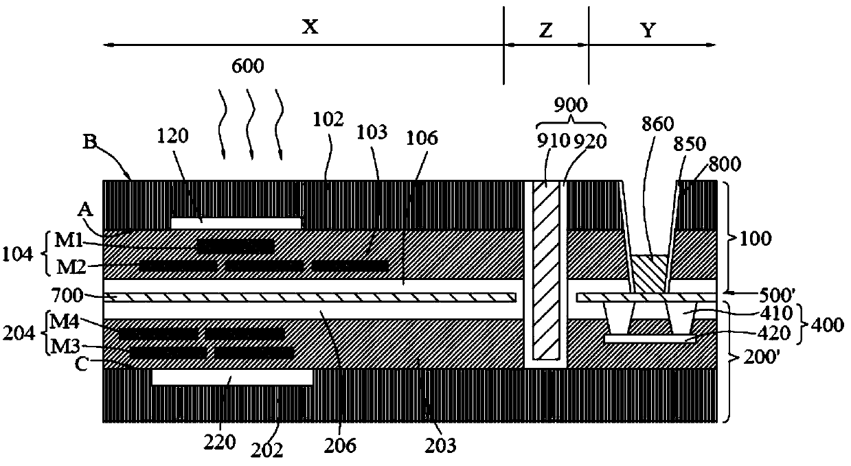
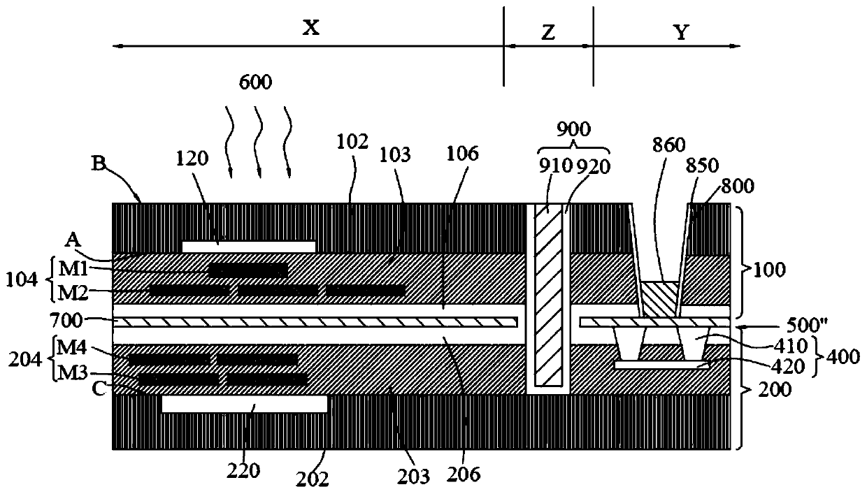
[0025] The following descriptions of the various embodiments refer to the accompanying drawings to illustrate specific embodiments in which the invention may be practiced. The directional terms mentioned in the present invention, such as [top], [bottom], [top], [bottom], [left], [right], [inside], [outside], [side], etc., are only for reference The orientation of the attached schema. Therefore, the directional terms used are used to illustrate and understand the present invention, but not to limit the present invention. In the figures, similar elements are denoted by the same reference numerals.

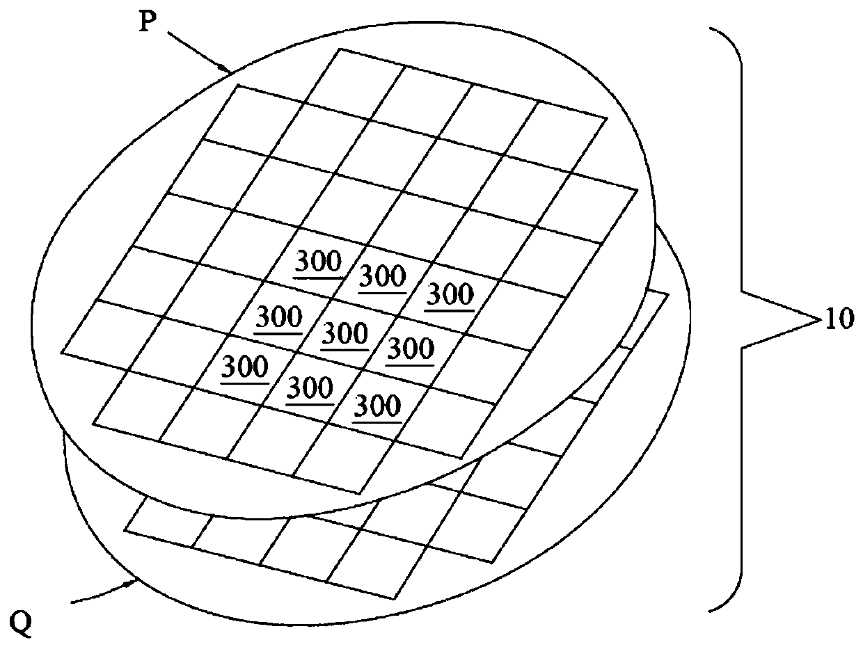
[0026] figure 1 is an exploded view of the three-dimensional integrated circuit 10 of the present invention. see figure 1 , the three-dimensional integrated circuit 10 is formed by stacking a first integrated circuit wafer (IC wafer) P and a second integrated circuit wafer Q. The first integrated circuit die P and the second integrated circuit die Q may include silicon, gallium ...


PUM


Abstract

The invention discloses a semiconductor device comprising a first substrate structure which comprises a first semiconductor element and a first dielectric layer located on the first semiconductor element; a second substrate structure including a second semiconductor element and a second dielectric layer on the second semiconductor element; and a multifunctional conductive layer positioned betweenthe first substrate structure and the second substrate structure; wherein the two sides of the multifunctional conducting layer are connected with the first dielectric layer and the second dielectriclayer respectively, projections of the first semiconductor element and the second semiconductor element on a set plane fall into projections of the multifunctional conducting layer on the set plane,and the set plane is perpendicular to the thickness direction of the first dielectric layer; as well as a lead-out structure used for receiving / outputting an electric signal, penetrates through the first substrate structure along the thickness direction and extends to be in local contact with the multifunctional conductive layer.

Description

technical field [0001] The invention relates to the technical field of semiconductor devices, and in particular to a three-dimensionally stacked semiconductor device containing a plurality of semiconductor devices. Background technique [0002] In the electronics industry, three-dimensional (3D) stacking technology significantly contributes to the integration of semiconductor devices. To form a 3D stack, two or more chips are arranged one on top of the other and bonded. [0003] 3D stacking technology offers many potential advantages, including such as improved form factor, lower cost, enhanced performance, and greater integration through system-on-chip (SOC) solutions. The SOC architecture formed by 3D stacking enables high bandwidth connectivity of stacked semiconductor devices such as logic circuits and dynamic random access memory (DRAM). [0004] However, the above-mentioned 3D stacking technology still has many deficiencies, such as the interference between the exter...

Claims


Application Information

Patent Timeline
IPC IPC(8): H01L23/552H01L23/48H01L27/146
CPCH01L23/552H01L23/481H01L27/14636H01L27/14634
Inventor 胡思平
Owner YANGTZE MEMORY TECH CO LTD
Why Eureka
Try Eureka