Anti-static protective film for wafer cutting and preparation method thereof

A protective film, anti-static technology, applied in the direction of circuits, electrical components, film/sheet adhesives, etc. If the voltage is too large, the effect of improving the fixing and picking efficiency can be achieved.

Active Publication Date: 2020-06-19
广东硕成科技股份有限公司
View PDF3 Cites 3 Cited by
  • Summary
  • Abstract
  • Description
  • Claims
  • Application Information

AI Technical Summary

Problems solved by technology

[0002] In the process of semiconductor wafer processing, especially in the process of picking up crystal grains after wafer dicing in the later stage of wafer packaging testing, it is often because the small grains after cutting are easy to generate static electricity during the process of peeling off the dicing film. Die functionality causes damage, resulting in reduced yield in subsequent tests
[0003] At present, there are some protective films with anti-static coating in the market to play the role of stable protection, but this current protective film is simply anti-static treatment on the surface of the material, and there will still be a large static voltage during use. Phenomenon, the use is limited in some fields of cutting electronic parts that require high static electricity
[0004] At present, the wafer dicing protective film generally includes thermal debonding protective film and UV debonding protective film. These protective films generally have a long storage time or high temperature. The small molecules of the adhesive layer will remain on the surface of the bonded object, causing pollution to the bonded object; in addition, the peel strength of the protective film produced in China is low before the viscosity is reduced, and the peel strength is high after the viscosity is reduced. Realize high-accuracy fixing and efficient picking

Method used


Image

  • Anti-static protective film for wafer cutting and preparation method thereof

Examples


preparation example Construction

[0042] A second aspect of the present invention provides a method for preparing the antistatic wafer dicing protective film, comprising the following steps:

[0043] (1) the first antistatic layer is bonded to one side of the substrate film, and the second antistatic layer is bonded to the other side of the substrate film;

[0044] (2) Coating the raw materials of the adhesion-reducing layer on the surface of the second antistatic layer, pre-baking, laminating with the release film layer, and curing to obtain the wafer dicing protective film.

[0045] Preferably, the preparation method of the antistatic wafer cutting protection film comprises the steps of:

[0046] (1) Laminate the first antistatic layer with the substrate film, and then with the second antistatic layer;

[0047] (2) Coating the treated raw material of the adhesion-reducing layer on the surface of the second antistatic layer, pre-baking, laminating with the release film layer, and curing to obtain the wafer d...
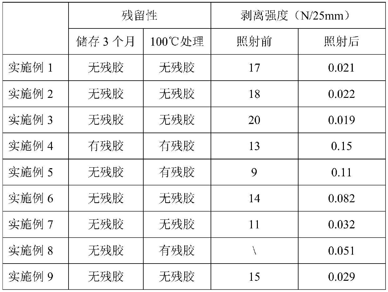
Embodiment 1

[0052] Embodiment 1 of the present invention provides an antistatic wafer dicing protective film, which sequentially includes a first antistatic layer, a substrate layer, a second antistatic layer, an adhesion-reducing layer, and a release film layer;

[0053] The debonding layer includes the following raw materials in parts by weight: 22 parts of acrylate monomers, 11 parts of acrylate oligomers containing active reactive groups, 1.0 parts of photoinitiators, 5 parts of fillers and 26 parts of solvents;

[0054] The acrylate monomers are butyl acrylate, lauric acrylate and 1,4-butanediol diacrylate, and the molar ratio of butyl acrylate, lauric acrylate and 1,4-butanediol diacrylate is 1: 0.21:0.32;

[0055] The raw materials for the preparation of the acrylate oligomer containing active reactive groups include hydroxyl-containing acrylate monomers and polyisocyanates, and the molar ratio of the hydroxyl groups in the hydroxyl-containing acrylate monomers to the isocyanate gr...

Embodiment 2

[0069] Embodiment 2 of the present invention provides an antistatic wafer dicing protective film, which sequentially includes a first antistatic layer, a substrate layer, a second antistatic layer, an adhesion-reducing layer, and a release film layer;

[0070] The debonding layer includes the following raw materials in parts by weight: 38 parts of acrylate monomers, 19 parts of acrylate oligomers containing active reactive groups, 4.0 parts of photoinitiators, 15 parts of fillers and 53 parts of solvents;

[0071] The acrylate monomers are butyl acrylate, lauric acrylate and 1,4-butanediol diacrylate, and the molar ratio of butyl acrylate, lauric acrylate and 1,4-butanediol diacrylate is 1: 0.35:0.49;

[0072] The raw materials for the preparation of the acrylate oligomer containing active reactive groups include hydroxyl-containing acrylate monomers and polyisocyanates, and the molar ratio of the hydroxyl groups in the hydroxyl-containing acrylate monomers to the isocyanate g...


PUM

PropertyMeasurementUnit
thicknessaaaaaaaaaa
thicknessaaaaaaaaaa
thicknessaaaaaaaaaa

Abstract

The invention provides an anti-static protective film for wafer cutting. The anti-static protective film sequentially comprises a first anti-static layer, a substrate layer, a second anti-static layer, a viscosity reduction layer and a release film layer. According to the invention, the protective film for wafer cutting is prepared by combining the double-sided antistatic layers and a viscosity reducing film material containing an antistatic filler, so the phenomenon of residual glue easily occurring in long-term storage or under a high-temperature condition is avoided; and meanwhile, the peeling strength of the protective film for wafer cutting before viscosity reduction can be improved, and the peeling strength of the protective film after viscosity reduction can be reduced, so accuratefixing and picking efficiency are improved.

Description

technical field [0001] The invention belongs to the technical field related to semiconductors, and more specifically, the invention provides an antistatic wafer cutting protection film and a preparation method thereof. Background technique [0002] In the process of semiconductor wafer processing, especially in the process of picking up crystal grains after wafer dicing in the later stage of wafer packaging testing, it is often because the small grains after cutting are easy to generate static electricity during the process of peeling off the dicing film. The functionality of the die causes damage, resulting in lower yields in subsequent testing. [0003] At present, there are some protective films with anti-static coating in the market to play the role of stable protection, but this current protective film is simply anti-static treatment on the surface of the material, and there will still be a large static voltage during use. Phenomenon, the use in some fields of cutting ...

Claims


Application Information

Patent Timeline
Patent Type & Authority Applications(China)
IPC IPC(8): C09J7/29C09J7/30C09J175/14C09J4/02C09J11/04H01L21/683
CPCC09J7/29C09J7/30C09J175/14C09J4/00C09J11/04H01L21/6836C09J2203/326C09J2475/00C09J2433/00C08K3/042
Inventor 柯跃虎诸葛锋曾庆明
Owner 广东硕成科技股份有限公司
Why Eureka
Try Eureka