Silicon wafer micro-crack detection device based on solar cell piece and using method thereof

A technology for solar cells and detection devices, which is applied in measuring devices, optical testing of flaws/defects, and material analysis through optical means. Reduce and other problems, to achieve the effect of strengthening the lighting effect

Pending Publication Date: 2020-06-23
EOPLLY NEW ENERGY TECH
View PDF6 Cites 2 Cited by
  • Summary
  • Abstract
  • Description
  • Claims
  • Application Information

AI Technical Summary

Problems solved by technology

[0004] At present, silicon wafer detection is included in the processing method of solar cells. In the prior art, when detecting whether there are cracks in the silicon wafer, it is usually to irradiate the silicon wafer with light, so as to detect whether the silicon wafer is transparent or not by observing whether it is transparent or not. There are cracks, but in the prior art, there may be small cracks in silicon wafers, which may prevent light from passing through the cracks, so that it is easy to make silicon wafers with cracks be regarded as qualified products, which may make silicon wafers made of Reduced energy conversion efficiency of solar cells

Method used


Image

  • Silicon wafer micro-crack detection device based on solar cell piece and using method thereof
  • Silicon wafer micro-crack detection device based on solar cell piece and using method thereof
  • Silicon wafer micro-crack detection device based on solar cell piece and using method thereof

Examples


Embodiment 1

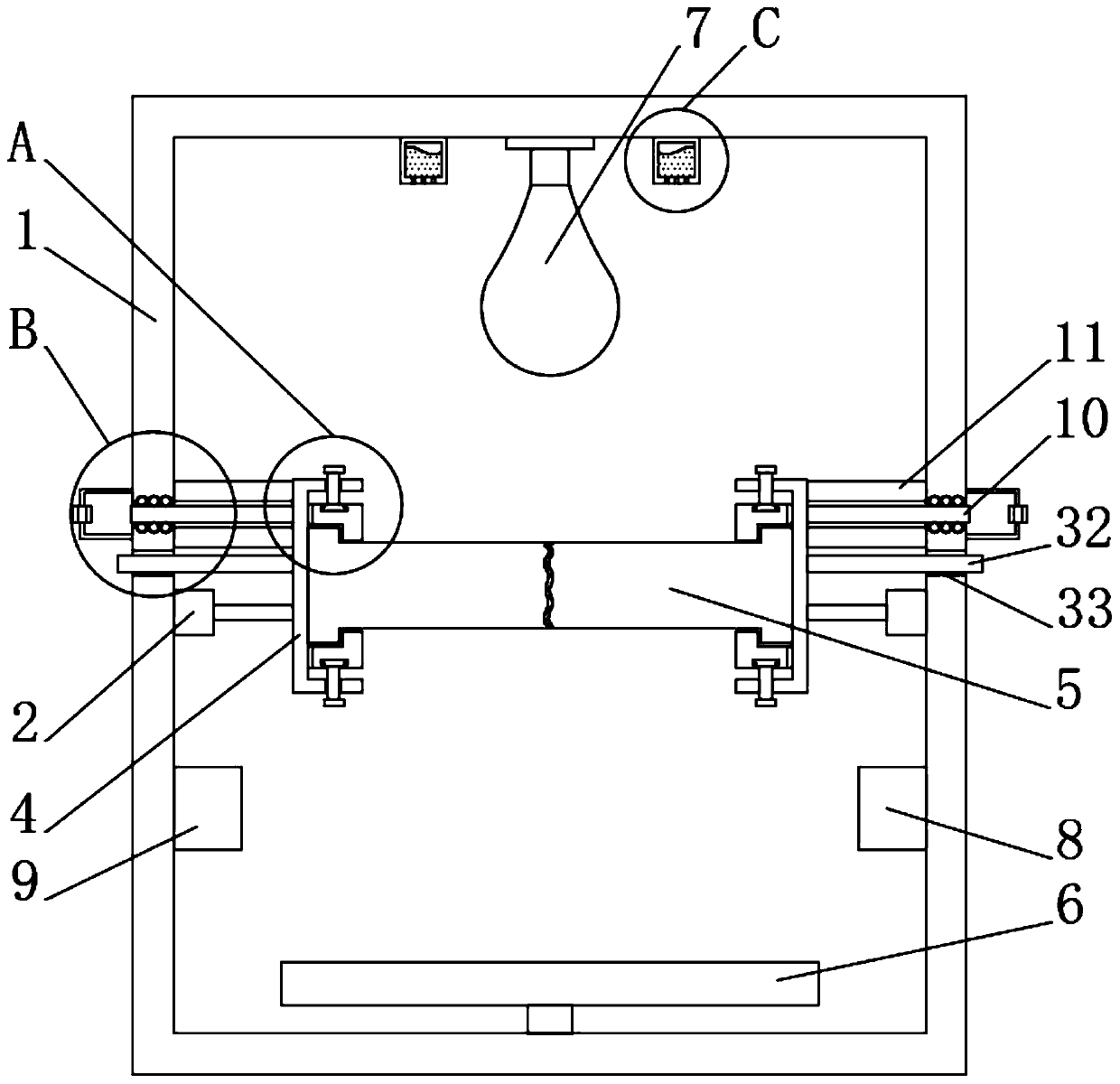
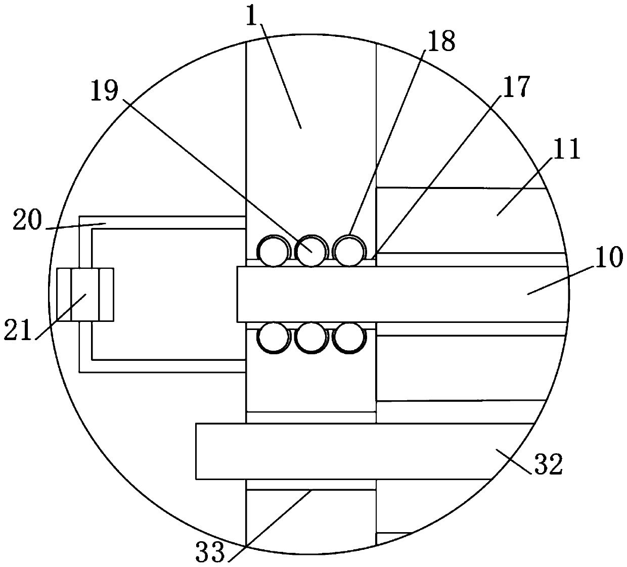
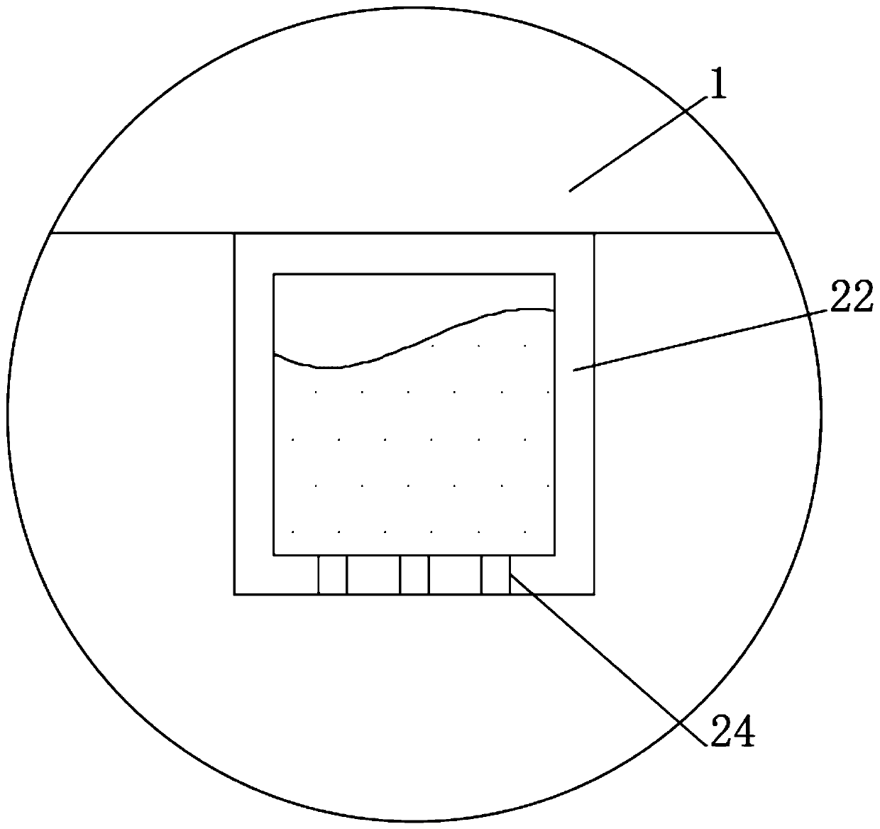
[0036] see Figure 1-2 , a micro-crack detection device based on solar cell silicon wafers, comprising a detection equipment main body 1, cylinders 2 are installed on the left and right inner walls of the detection equipment main body 1, the output ends of the two cylinders 2 are fixedly connected with clamping equipment 4, two A silicon wafer 5 is arranged between the clamping equipment 4, a photoelectric sensor 6 is installed at the inner bottom of the detection equipment main body 1, an LED light 7 is installed on the upper inner wall of the detection equipment main body 1, a power supply 8 is installed on the right inner wall of the detection equipment main body 1, and the detection equipment A controller 9 is installed on the left inner wall of the main body 1, a movable plate 10 is fixedly connected to the ends of the two holding devices 4 away from each other, an annular bag 11 is fixedly connected between the holding device 4 and the inner wall of the main body 1 of the...


PUM


Abstract

The invention discloses a silicon wafer micro-crack detection device based on a solar cell piece and a using method thereof, and belongs to the technical field of solar cell sheets. According to the scheme, a silicon wafer is continuously in a stretching-compressing-stretching change state by controlling an air cylinder; light irradiated by an LED lamp penetrates through cracks and then is received by a photoelectric sensor; a movable plate is enabled to translate left and right in a first through hole; an annular bag is repeatedly extruded; friction ball cavities in the inner air bag rub witheach other; the friction ball cavities expand after being heated; mercury in a transparent liquid bag is expanded; the transparent liquid bag has a certain light reflecting effect; heat is generatedthrough a semiconductor chilling plate so that a temperature and pressure intensity of an upper side of a detection equipment main body are improved; and melting of ice slags in a second mounting frame is accelerated, generated water drops drop onto the silicon wafer, the water drops penetrate through the cracks along with an airflow, the water drops are attached to peripheries of the cracks in alower side surface, and positions of the cracks are conveniently marked.

Description

technical field [0001] The invention relates to the technical field of solar cells, and more specifically, relates to a detection device for micro-cracks in silicon wafers based on solar cells and a method for using the same. Background technique [0002] Solar energy is a kind of renewable energy. It refers to the thermal radiation energy of the sun. Its main performance is the sun's rays, which are often used to generate electricity or provide energy for water heaters in modern times. The heat radiation can survive, and since ancient times, humans have also known to use sunlight to dry objects and use it as a method of making food, such as making salt and drying salted fish. In the case of decreasing fossil fuels, solar energy has become an important source of energy for human beings. It is an integral part and has been continuously developed. There are two ways to use solar energy: photothermal conversion and photoelectric conversion. Solar power is a new type of renewabl...

Claims


Application Information

Patent Timeline
Patent Type & Authority Applications(China)
IPC IPC(8): G01N21/95G01N21/01
CPCG01N21/9505G01N21/01
Inventor 汤叶华徐永峰王孟施成军
Owner EOPLLY NEW ENERGY TECH
Why Eureka
Try Eureka