N-type fragmented solar cell structure and manufacturing method thereof

A technology of a solar cell and a manufacturing method, which is applied in the field of solar cells, can solve the problems such as the reduction of the efficiency of the sliced ​​cell, and achieve the effects of edge recombination suppression and FF improvement.

Inactive Publication Date: 2020-06-23
苏州光汇新能源科技有限公司
View PDF10 Cites 12 Cited by
  • Summary
  • Abstract
  • Description
  • Claims
  • Application Information

AI Technical Summary

Problems solved by technology

Due to the influence of the above-mentioned edge recombination of the slices, the efficiency of the sliced ​​batteries prepared by various batteries will decrease.
The general trend is that the cell with better surface passivation is more sensitive to the influence of edge recombination, and the reduction in efficiency after fragmentation is greater; for example, the efficiency reduction of half-cell P-type PERC cells can usually be controlled within 0.1% abs , while the efficiency of the half-chip N-type heterojunction and TOPCON cells usually drops by 0.2-0.5% abs; in addition, for the same battery, the larger the ratio of the edge perimeter of the sliced ​​cell to the cell area, the greater the efficiency of the sliced ​​cell. The efficiency drop is also greater; for example, the efficiency drop of N-type heterojunction cells can reach about 1% abs

Method used


Image

  • N-type fragmented solar cell structure and manufacturing method thereof
  • N-type fragmented solar cell structure and manufacturing method thereof
  • N-type fragmented solar cell structure and manufacturing method thereof

Examples


preparation example Construction

[0054] Specifically, see Figure 5a , Figure 5b A method for preparing an N-type sliced ​​solar cell structure provided by an embodiment of the present invention includes the following steps:

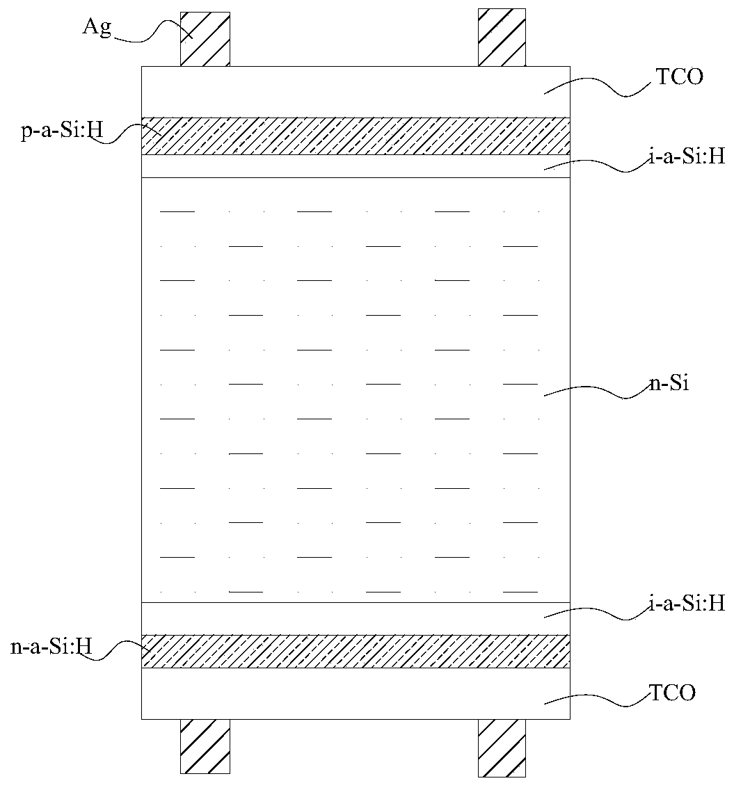
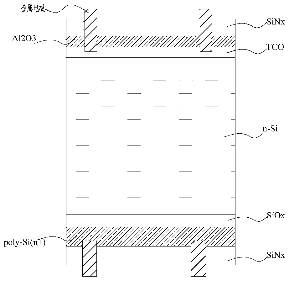
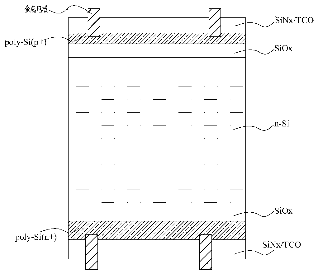
[0055] 1) Provide an N-type silicon wafer with a resistivity of 0.1-3Ω·cm, and process the N-type silicon wafer by laser cutting at the position corresponding to the slice on the first surface of the N-type silicon wafer to form a groove for the split, The width of the groove is 0.2-10um, preferably 0.2-1um; the depth of the groove is 0.5-50um, preferably 0.5-15um, and then a laminated passivation layer is deposited on the first surface, and the laminated passivation layer and N Type silicon wafers form heterogeneous p-n junctions;

[0056] If the battery is an N-type heterojunction battery, the stack passivation layer is i-a-Si:H / p-a-Si:H / TCO stack, where i-a-Si:H is 1-10nm thick, which is chemical passivation layer, p-a-Si:H thick 1-15nm is the field passivation layer, TCO is the ...

Embodiment 1

[0063] Example 1 Process of bisecting N-type heterojunction cells

[0064] 1) Provide N-type silicon wafers with a resistivity of 0.1-3Ω·cm;

[0065] 2) On the first surface of the N-type silicon wafer and located at 1 / 2 of the side length, a kerf is formed by laser irradiation, the width of the kerf is 0.2-10um, preferably 0.2-1um; the kerf The depth is 0.5-50um, preferably 0.5-15um;

[0066] 3) Surface treatment of the N-type silicon wafer with an alkaline solution to remove the damaged layer, and then the N-type silicon wafer is cleaned and textured. After cleaning, the silicon wafer is required to be free of spots, scratches, water marks, etc.;

[0067]4) Deposit the laminated intrinsic hydrogenated amorphous silicon film (i-a-Si:H) and N-type hydrogenated amorphous silicon film (n-a-Si:H) on the second surface of the N-type silicon wafer by PECVD or hot wire CVD -Si:H);

[0068] 5) Using PECVD or hot wire CVD to deposit a laminated intrinsic hydrogenated amorphous sili...

Embodiment 2

[0084] Example 2 Six equal slices of N-type heterojunction cells

[0085] 1) Provide N-type silicon wafers with a resistivity of 0.1-3Ω·cm;

[0086] 2) The first surface of the N-type silicon wafer is located at 1 / 6 of the side length, and 5 grooves are formed by laser irradiation. The width of the groove is 0.2-10um, preferably 0.2-1um; the depth of the groove is 0.5-50um, preferably 0.5-15um.

[0087] 3) Surface treatment of the N-type silicon wafer with an alkaline solution to remove the damaged layer, and then the N-type silicon wafer is cleaned and textured. After cleaning, the silicon wafer is required to be free of spots, scratches, water marks, etc.;

[0088] 4) Using PECVD or hot wire CVD to deposit stacked intrinsic hydrogenated amorphous silicon films (i-a-Si:H) and N-type hydrogenated amorphous silicon films (n-a- Si:H);

[0089] 5) Deposit a laminated intrinsic hydrogenated amorphous silicon film (i-a-Si:H) and a P-type hydrogenated amorphous silicon film (p-a-...


PUM

PropertyMeasurementUnit
thicknessaaaaaaaaaa
thicknessaaaaaaaaaa
thicknessaaaaaaaaaa

Abstract

The invention discloses an N-type fragmented solar cell structure and a manufacturing method thereof. The manufacturing method comprises: providing an n-type solar cell substrate, and processing at least one side surface of the substrate to form a cutting groove for cracking; at least forming a continuous passivation layer on the surface of one side of the substrate, and enabling the grooving wallof the grooving to be covered by the passivation layer; splitting the substrate along the cutting groove to form a fragmented battery, and forming a natural oxide layer on the quasi-neutral region, which is not covered by the passivation layer, of the edge of the fragmented battery; and passivating the quasi-neutral region, which is not covered by the passivation layer, of the edge of the fragmented battery and the natural oxide layer by using hydrogen plasma. According to the invention, the first passivation structure and the second passivation structure are formed on the edge of the fragmented cell after slicing, the first passivation structure covers the exposed space charge region, and the second passivation structure covers the quasi-neutral region, so that the fragmented cell with the edge full-area passivation structure is obtained.

Description

technical field [0001] The invention relates to a manufacturing method of a solar cell, in particular to an N-type sliced ​​solar cell structure and a manufacturing method thereof, and belongs to the technical field of solar cells. Background technique [0002] N-type solar cells are considered to be a more efficient solar cell technology after P-type PERC cells. Among them, N-type heterojunction cells and N-type TOPCON cells are the two most promising cell technologies to achieve low cost and high efficiency. The N-type heterojunction cell has a double-sided passivation contact structure, which has the advantages of good passivation effect, low process temperature, and double-sided power generation. [0003] The basic structure of an N-type heterojunction cell is as follows: figure 1 As shown, the intrinsic hydrogenated amorphous silicon film (i-a-Si:H) / p-type hydrogenated amorphous silicon film (p-a-Si:H) stack and the intrinsic hydrogenated amorphous silicon film ( i-a-...

Claims


Application Information

Patent Timeline
Patent Type & Authority Applications(China)
IPC IPC(8): H01L31/18H01L31/042
CPCH01L31/042H01L31/1804H01L31/1868Y02E10/547Y02P70/50
Inventor 杨黎飞杨青松李杏兵张闻斌
Owner 苏州光汇新能源科技有限公司
Why Eureka
Try Eureka