
Metal transparent electrode and organic solar cell

A solar cell and transparent electrode technology, applied in the field of solar cells, can solve problems such as poor flexibility, high preparation cost, and fragile transparent electrode materials, and achieve high photocurrent, improve light utilization, and improve transmission and collection efficiency.

Active Publication Date: 2020-06-23
HANGZHOU DIANZI UNIV
View PDF18 Cites 1 Cited by
  • Summary
  • Abstract
  • Description
  • Claims
  • Application Information

AI Technical Summary

Problems solved by technology

[0005] The present invention provides a novel flexible metal transparent electrode with high conductivity and high transmittance in order to overcome the problems of fragile, poor flexibility and high preparation cost of the conventional transparent electrode materials commonly used in organic solar cells

Method used


Image

  • Metal transparent electrode and organic solar cell
  • Metal transparent electrode and organic solar cell
  • Metal transparent electrode and organic solar cell

Examples


Embodiment 1

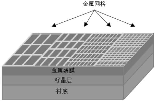
[0032] The glass substrate was ultrasonically cleaned with detergent, isopropanol, ethanol, and acetone in sequence, and dried with nitrogen after cleaning; a ZnO film was prepared on the surface of the glass substrate by spin coating with a thickness of about 45 nm; A layer of 5 nm ultra-thin Ag film was vacuum evaporated on the surface; then the thicknesses of 10 nm, 15 nm, 20 nm, and 25 nm were evaporated on it, and the corresponding inscribed circle diameters were 200 μm, 150 μm, 100 μm, 50 μm, Ag grid with a line width of 5 μm, formed as figure 1 A metallic transparent electrode with a conductivity step distribution shown.

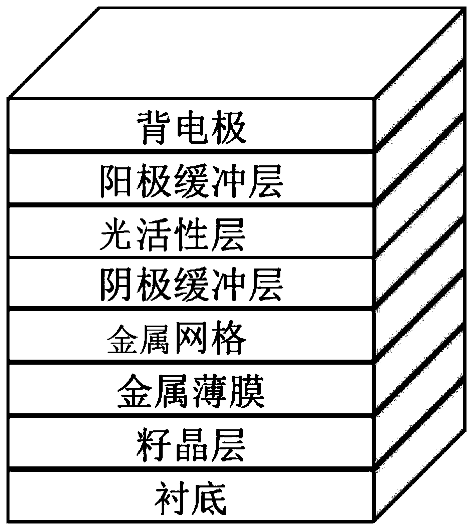
[0033] Spin-coating 30 nm of SnO on the surface of transparent metal electrodes 2 (cathode buffer layer), and anneal the formed film at 150 °C for 10 minutes; then spin-coat PTB7-Th and PC 71 Mixed solution of BM, PTB7-Th and PC 71 The mass ratio of BM was 1:1.5, and a layer of PTB7-Th and PC with a thickness of 90 nm was obtained 71 BM hybrid fil...

Embodiment 2

[0035] The glass substrate was ultrasonically cleaned with detergent, isopropanol, ethanol, and acetone in sequence, and dried with nitrogen after cleaning; MoO was prepared on the surface of the glass substrate by spin coating 3 thin film with a thickness of about 40 nm; then in MoO 3 A layer of 5 nm ultra-thin Au film was vacuum evaporated on the surface of the film; then the thicknesses of 10 nm, 15 nm, 20 nm, and 25 nm were evaporated on it, and the corresponding inscribed circle diameters were 200 μm, 150 μm, and 100 μm , 50 μm, step-structured Ag grid with a line width of 5 μm, formed as figure 1 A metallic transparent electrode with a conductivity step distribution shown.

[0036]Spin-coat 30 nm of Bphen (cathode buffer layer) on the surface of the transparent metal electrode, and anneal the formed film at 150 °C for 10 minutes; then spin-coat P3HT and PC 71 Mixed solution of BM, PTB7-Th and PC 71 The mass ratio of BM was 1:1.5, and a layer of PTB7-Th and PC with a t...

Embodiment 3

[0038] The glass substrate was ultrasonically cleaned with detergent, isopropanol, ethanol, and acetone in sequence, and dried with nitrogen after cleaning; TeO2 was prepared on the surface of the glass substrate by spin coating. 2 thin film with a thickness of about 50 nm; then in TeO 2 A layer of 5 nm ultra-thin Cu film was vacuum-evaporated on the surface of the film; then, the thicknesses of 10 nm, 15 nm, 20 nm, and 25 nm were evaporated on it, and the corresponding inscribed circle diameters were 200 μm, 150 μm, and 100 μm. , 50 μm, step-structured Ag grid with a line width of 5 μm, formed as figure 1 A metallic transparent electrode with a conductivity step distribution shown.

[0039] Spin-coat 30 nm of PFN-Br (cathode buffer layer) on the surface of the transparent metal electrode, and anneal the formed film at 150 °C for 10 minutes; then spin-coat PTB7 and PC 71 Mixed solution of BM, PTB7-Th and PC 71 The mass ratio of BM was 1:1.5, and a layer of PTB7-Th and PC wi...


PUM

PropertyMeasurementUnit
thicknessaaaaaaaaaa
diameteraaaaaaaaaa
widthaaaaaaaaaa

Abstract

The invention relates to the technical field of solar cells, and particularly relates to a metal transparent electrode and an organic solar cell. The metal transparent electrode sequentially comprisesa seed crystal layer, a metal film and a metal grid from bottom to top, wherein the metal grid is of a stepped structure with conductivity increasing progressively. According to the metal transparentelectrode, a metal film / metal grid composite structure is adopted, the capture of incident light can be enhanced by utilizing an optical resonance microcavity effect formed between the metal film andthe back electrode on the one hand so as to obtain high photocurrent; and on the other hand, in allusion to the problem of non-uniform distribution of the carrier collection efficiency in the large-area device, the transmission and collection efficiency of the carriers in the large-area device is improved by preparing the metal grid with the conductivity distributed in a stepped mode on the metalfilm.

Description

technical field [0001] The invention relates to the technical field of solar cells, in particular to a metal transparent electrode and an organic solar cell. Background technique [0002] The device efficiency of organic solar cells has reached the standard for commercialization, but how to effectively convert the small-area devices in the laboratory into large-area modules and how to obtain high-efficiency large-area device modules has become a crucial issue. [0003] However, as the cell area increases, the photovoltaic properties of the device decrease significantly. This is because in a large-area device, the transmission distance of carriers in the horizontal direction increases, and the transmission efficiency is unevenly distributed. When the conductivity of the electrode is poor, the series resistance of the device will increase significantly, causing the carrier The collection efficiency is reduced, which in turn affects the performance of large-area devices. [0...

Claims


Application Information

Patent Timeline
Patent Type & Authority Applications(China)
IPC IPC(8): H01L51/44H01L51/42
CPCH10K30/00H10K30/82Y02E10/549
Inventor 臧月陈岭风辛青林君
Owner HANGZHOU DIANZI UNIV
Learn More