Photonic crystal high-power laser and preparation method thereof

A technology of high-power lasers and photonic crystals, applied in semiconductor lasers, lasers, phonon exciters, etc., can solve problems such as poor beam quality and limit the application of semiconductor lasers, and achieve wide wavelength tuning range, high power, and improved tuning range Effect

Active Publication Date: 2020-06-26
Shandong Huaguang Optoelectronics Co. Ltd.
View PDF7 Cites 1 Cited by
  • Summary
  • Abstract
  • Description
  • Claims
  • Application Information

AI Technical Summary

Problems solved by technology

The beam quality of semiconductor lasers is still poor at present, and this shortcoming greatly limits the application of semiconductor lasers. It is widely used in fields such as laser welding that only require low beam quality but require high power.

Method used


Image

  • Photonic crystal high-power laser and preparation method thereof
  • Photonic crystal high-power laser and preparation method thereof

Examples


Embodiment 1

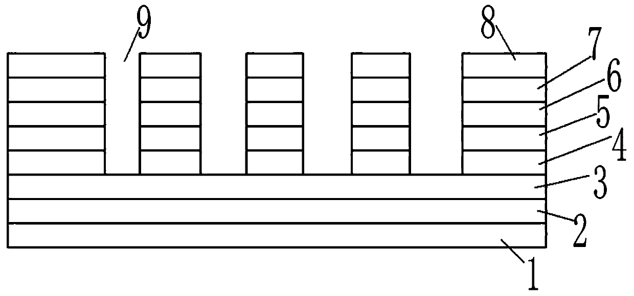
[0034] Further, the cross section of the air column 9 is circular, oval or polygonal.

[0035]A method for preparing a photonic crystal high-power laser, comprising the steps of:

[0036] a) Put the GaAs substrate into the growth chamber of the MOCVD equipment, and pass through , baked for 30 minutes in an environment with a temperature of 700±20°C, and after the , remove water and oxygen on the surface of the substrate to complete the heat treatment of the substrate surface;

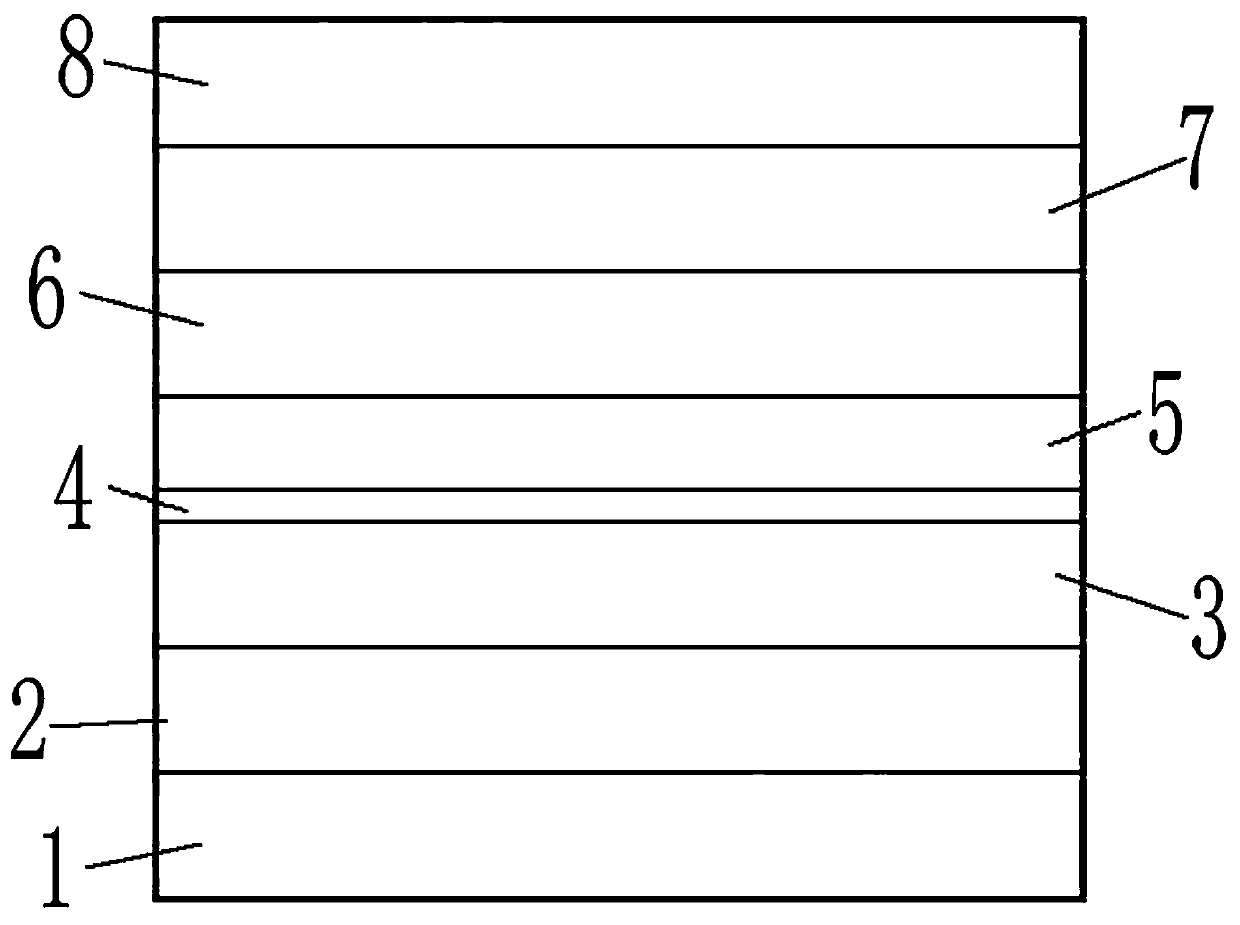
[0037] b) Lower the temperature to 650±20°C and pass through and TMGa, growing a GaAs low-temperature buffer layer 1 with a thickness of 0.5-1 μm on the GaAs substrate;

[0038] c) The temperature is maintained at 650±20°C, and the , TMGa and TMAl, growing an AlGaAs lower confinement layer 2 on the GaAs low-temperature buffer layer 1;

[0039] d) The temperature is kept at 650±20°C, and the lower Bragg reflective layer 3 made of n-type AlxGayAs / AlxGayAs is grown on the AlGaAs lower confinemen...

Embodiment 2

[0048] Preferably, when growing the GaAs low-temperature buffer layer 1 in step b), the doping concentration in the growth chamber of the MOCVD equipment is 1E17-5E18 atoms / , when growing the AlGaAs lower confinement layer 2 in step c), the doping concentration in the growth chamber of the MOCVD equipment is 1E17-5E18 atoms / .

Embodiment 3

[0050] Preferably, the thickness of the lower Bragg reflective layer 3 in step d) is 0.5-2 μm, and the doping concentration in the growth chamber of the MOCVD equipment when growing the lower Bragg reflective layer 3 is 1E16-5E17 atoms / , when growing the lower Bragg reflection layer 3, cyclic growth is adopted, and the number of cycles is 20-30 times.


PUM

PropertyMeasurementUnit
thicknessaaaaaaaaaa
thicknessaaaaaaaaaa
thicknessaaaaaaaaaa

Abstract

The invention discloses a photonic crystal high-power laser preparation method. The method comprises the following steps: adding an isolation layer between a quantum well light-emitting layer and a lower Bragg reflection layer; after the epitaxial wafer is grown, carrying out laser etching to form an air column to form a photonic crystal, wherein the photons generated by work of the quantum well light-emitting layer can only pass through the surface of the photonic crystal through a resonance tunnel effect, and a wider harmonizing range and a narrower line width can be effectively improved; integrating a lower Bragg emitting layer and an upper Bragg reflecting layer in one laser to form two independent gratings, so that a wider wavelength harmonizing range, narrower spectral line width andhigher power are realized, and stimulated radiation light and external light causing stimulated radiation have the same frequency, phase, polarization and propagation direction. Through stimulated radiation, homomorphic photon number amplification can be realized so as to obtain coherent light with extremely high photon degeneration degree. Due to the fact that the power of an existing laser is generally low, long-distance and multi-path laser application can be achieved through high power.

Description

technical field [0001] The invention relates to the technical field of optoelectronic manufacturing, in particular to a photonic crystal high-power laser and a preparation method thereof. Background technique [0002] Due to their small size, low degradation rate, long-term use and high electro-optical conversion efficiency, semiconductor lasers are widely used in the application field, involving long-distance optical fiber signal transmission, welding processing and many other fields [16- twenty three]. [0003] The most important application of semiconductor lasers is optical fiber communication, which has very strict requirements on the spectrum of the light source. For this reason, people add a modulating periodic mechanism, such as a distributed Bragg reflection structure, in the longitudinal direction of the laser. Narrow linewidth distributed feedback Bragg diode laser (DFB-LD) is used for optical fiber communication, and the single channel code rate can reach 10Gb / ...

Claims


Application Information

Patent Timeline
Patent Type & Authority Applications(China)
IPC IPC(8): H01S5/343H01S5/187
CPCH01S5/187H01S5/343H01S5/34346
Inventor 李志虎于军邓桃朱振
Owner Shandong Huaguang Optoelectronics Co. Ltd.
Why Eureka
Try Eureka