Separation method of metal substrate light-emitting device wafer

A technology for metal substrates and light-emitting devices, applied in semiconductor devices, semiconductor/solid-state device manufacturing, electrical components, etc., can solve the problems of metal slag easily splashing into the light-emitting area, increase device leakage, etc., and achieve multi-chip output, The effect of reducing yield loss

Inactive Publication Date: 2020-07-03
西安唐晶量子科技有限公司
View PDF5 Cites 0 Cited by
  • Summary
  • Abstract
  • Description
  • Claims
  • Application Information

AI Technical Summary

Problems solved by technology

However, due to the high power of the laser cutting metal substrate, the temperature of the laser ablation area is very high instantaneously, and the gap between the light-emitting devices is generally designed to be tens of microns to more than one hundred microns due to cost factors, and the heat in the ablation area Conducted over a short distance of tens of microns on the surface of the substrate, resulting in a higher temperature in the light-emitting area. In addition, metal debris from laser cutting is easy to splash into the light-emitting area, which increases the risk of device leakage. When laser cutting the front side, it is usually coated Protective fluid to reduce the risk of splashing metal residue from laser ablation, but it cannot be completely avoided

Method used


Image

  • Separation method of metal substrate light-emitting device wafer
  • Separation method of metal substrate light-emitting device wafer
  • Separation method of metal substrate light-emitting device wafer

Examples


Embodiment Construction

[0012] The present invention will be further described in detail below in conjunction with specific embodiments, which are explanations of the present invention rather than limitations.

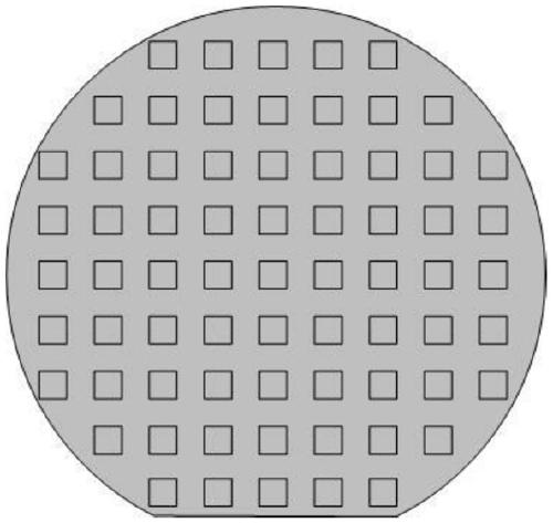
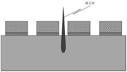
[0013] Usually, the light-emitting chip pattern existing on the front of the wafer can provide a reference for the scribing path of the laser, while the back is usually smooth and has no pattern. The feature of the present invention is that an auxiliary pattern is formed on the back of the metal substrate in combination with the pattern on the front of the substrate. It is used to guide the movement of the laser, and the laser is ablated at a suitable position on the back, and then aligned with the laser ablation line on the back, and splits on the front.

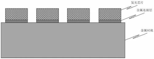
[0014] The first step is to provide a GaN-based light-emitting chip wafer with a WCu substrate. The structure includes: a 210um thick WCu substrate, a metal connection layer composed of Au, Sn, and Ti, and a GaN-based light-emitting chip; ...


PUM

PropertyMeasurementUnit
wavelengthaaaaaaaaaa

Abstract

The invention discloses a separation method of a metal substrate light-emitting device wafer. The method comprises the steps that a metal substrate is provided, the front face of the substrate is connected with a light-emitting device array through a metal connecting layer, an auxiliary pattern is formed on the back face of the metal substrate, a laser beam is focused on the back face of the substrate, the back face of the substrate is ablated under the guidance of the auxiliary pattern, splitting is conducted on the front face of the substrate along gaps of the light-emitting array, and light-emitting devices are separated. Due to the fact that laser is cut on the back face, the influence of the laser on the front-face light-emitting device is small, and yield loss caused by laser cuttingcan be reduced.

Description

technical field [0001] The invention relates to a preparation process of a light-emitting device on a metal substrate, in particular to a method for separating a wafer of a light-emitting device on a metal substrate. Background technique [0002] Because of its good thermal conductivity, ductility and electrical conductivity, metal substrates have certain applications in vertical structure light-emitting devices. At present, metal substrate vertical structure LEDs perform well under high current conditions. It is widely used in the lighting market. After the light-emitting device is prepared, the device on the metal substrate needs to be separated. This separation method has an important impact on the yield of the device. [0003] For wafers with metal substrates, the method of laser cutting the front side of the wafer is generally used to separate devices, such as image 3 with Figure 4 shown. However, due to the high power of the laser cutting metal substrate, the tempe...

Claims


Application Information

Patent Timeline
Patent Type & Authority Applications(China)
IPC IPC(8): H01L21/78H01L33/00
CPCH01L21/78H01L33/0066H01L33/0075
Inventor 龚平吴旗召
Owner 西安唐晶量子科技有限公司
Why Eureka
Try Eureka