Method for preparing OLED device by femtosecond laser forward transfer technology

A femtosecond laser and femtosecond laser technology are applied in the fields of electrical solid-state devices, semiconductor devices, semiconductor/solid-state device manufacturing, etc., and can solve problems such as good effect and high cost

Inactive Publication Date: 2020-07-07
WUHAN UNIV OF TECH
View PDF4 Cites 0 Cited by
  • Summary
  • Abstract
  • Description
  • Claims
  • Application Information

AI Technical Summary

Problems solved by technology

The OLED evaporated by FMM method is very good, and the three primary colors are very pure, but the cost is very high

Method used


Image

  • Method for preparing OLED device by femtosecond laser forward transfer technology
  • Method for preparing OLED device by femtosecond laser forward transfer technology
  • Method for preparing OLED device by femtosecond laser forward transfer technology

Examples


Embodiment Construction

[0026] In order to make the object, technical solution and advantages of the present invention clearer, the present invention will be further described in detail below in conjunction with the accompanying drawings and embodiments. It should be understood that the specific embodiments described here are only used to explain the present invention, not to limit the present invention.

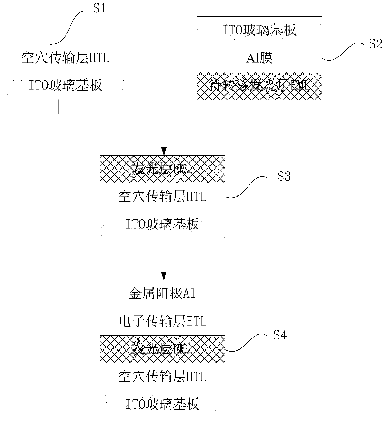
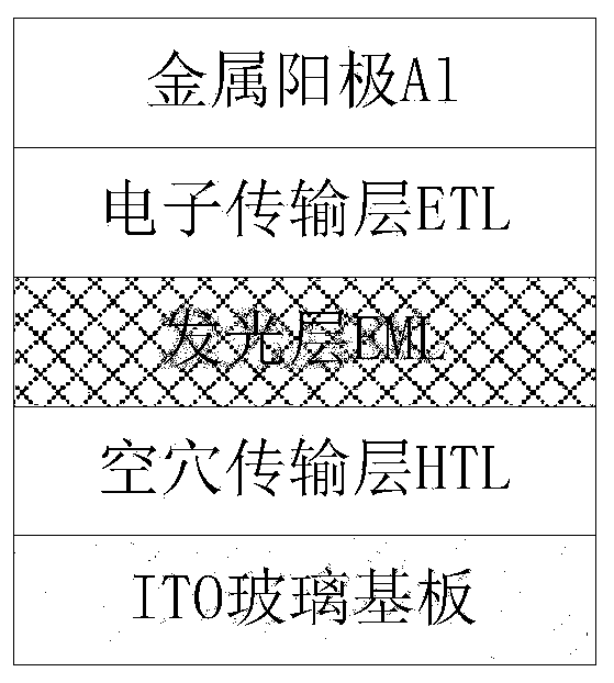
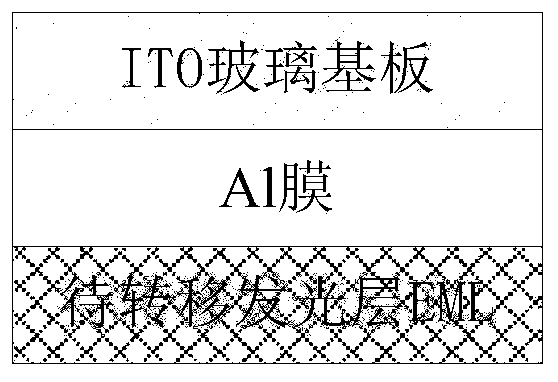
[0027] Such as figure 1 As shown, the present invention provides a method for preparing an OLED light-emitting device by femtosecond laser front transfer technology. The prepared OLED light-emitting device includes an ITO (indium tin oxide semiconductor) glass substrate and a hole transport layer that are stacked sequentially from bottom to top. HTL, light emitting layer EML, electron transport layer ETL and metal anode Al, comprising the following steps:

[0028] S1. Evaporating a hole transport layer HTL on an ITO glass substrate to form an acceptor ITO glass substrate, the thickness of the hole...


PUM

PropertyMeasurementUnit
thicknessaaaaaaaaaa
thicknessaaaaaaaaaa
thicknessaaaaaaaaaa

Abstract

The invention discloses a method for preparing an OLED device by a femtosecond laser forward transfer technology, and the method comprises the following steps: evaporating a hole transport layer HTL on an ITO glass substrate to form an acceptor ITO glass substrate; then preparing a donor ITO glass substrate of a to-be-transferred light-emitting layer EML with a specific pattern; then transferringa light-emitting layer EML on the donor ITO glass substrate to the hole transport layer HTL in the step S1 by using femtosecond laser pulses; and finally, evaporating an electron transport layer ETL and a metal anode Al on the transferred light-emitting layer EML. According to the method, the organic light-emitting functional layer thin film material can be accurately transferred to the corresponding substrate in a high-resolution and specific shape under the non-vacuum condition, accurate control over the transfer area is achieved, the requirement for the machining environment is low, the cost is reduced, and meanwhile, the production efficiency is improved.

Description

technical field [0001] The invention relates to the field of laser processing, in particular to a method for preparing an OLED light-emitting device by femtosecond laser front transfer technology. Background technique [0002] The full name of OLED is Organic Light-Emitting Diode, and the Chinese name is Organic Light-Emitting Diode. Compared with the widely used flat-panel display LCD, OLED has the characteristics of active light emission, high contrast, ultra-thin, low temperature resistance, fast response, low power consumption, wide viewing angle, strong shock resistance, etc., and is more suitable for flexible display and 3D show. [0003] At present, in the mainstream OLED manufacturing process, the solution to realize the full-color color of the OLED screen is mainly "evaporation". The technology used in this type of evaporation is called FMM (Fine Metal Mask), which is to cover a mask in order to distinguish pixels during evaporation, and the alignment of the mask ...

Claims


Application Information

Patent Timeline
Patent Type & Authority Applications(China)
IPC IPC(8): H01L51/56H01L51/00
CPCH10K71/18H10K71/00
Inventor 黄福志吕雪辉谭光耀王学文程一兵
Owner WUHAN UNIV OF TECH
Why Eureka
Try Eureka