Process method for depositing and doping surface of silicon wafer

A process method and technology on the surface of silicon wafers, applied in the field of deposition and doping processes, can solve problems such as uneven concentration, uneven film thickness, and poor uniformity, and achieve increased doping concentration, uniform film thickness between sheets, and consistent reactions Effect

Inactive Publication Date: 2020-07-10
LAPLACE RENEWABLE ENERGY TECH CO LTD
View PDF5 Cites 2 Cited by
  • Summary
  • Abstract
  • Description
  • Claims
  • Application Information

AI Technical Summary

Problems solved by technology

[0004] It is generally understood that in order to make the reaction more uniform or to make the reaction results such as film thickness and uniformity better, the gas will be mixed as uniformly as possible to achieve the above purpose, but the mixed gas is used for the reaction On the contrary, it will lead to poorer uniformity. The reasons are mainly the following two aspects. First, silane and dopant source gas enter the furnace body at the same time, and the gas concentration in each part is different, that is, the two gases react less near the outlet of the furnace. Intensive, and, due to the different decomposition rates of the blocked gas, during the operation of the gas in the furnace tube, due to the difference in the decomposition rate, the decomposition in the mixed gas is relatively fast and easily consumed in the first half, and in the second half. If the amount is reduced and the decomposition is relatively slow, the reaction is mainly carried out in the second half. This method will cause the problem of uneven film thickness and uneven concentration. In the prior art, the method of supplementing gas is usually used to solve this problem, but In fact, qi supplementation cannot fundamentally solve the above problems

Method used


Image

  • Process method for depositing and doping surface of silicon wafer
  • Process method for depositing and doping surface of silicon wafer
  • Process method for depositing and doping surface of silicon wafer

Examples


Embodiment 1

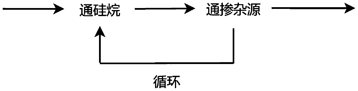
[0033] Take LPCVD doping as an example:

[0034] (1) Prepare 10 polished slices, 5 slices in group A grow a 100nm oxide layer, and 5 slices in group B are cleaned with hydrofluoric acid. (Group A is used to measure the film thickness of intrinsic silicon, group B is used to test the doping concentration, the same below)

[0035] (2) In the LPCVD furnace cavity, place a quartz boat, and put down a group A and a group B silicon wafer at 5 average intervals in the boat from the furnace mouth to the furnace tail (positions are respectively numbered 1, 2, 3, 4 , 5).

[0036] (3) Oxygen is introduced into the LPCVD furnace, and a layer of 1.5nm oxide layer is first grown on the surface of the silicon wafer.

[0037] (4) Evacuate oxygen and check for leaks.

[0038] (5) Control the temperature to 550°C and the pressure to 200mtorr, and start the aeration reaction;

[0039] The specific ventilation steps are:

[0040] (5.1) Pass into 300sccm silane, the ventilation time is 60 sec...

Embodiment 2

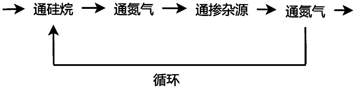
[0050] Take LPCVD doping as an example:

[0051] (1) Prepare 10 polished slices, 5 slices in group A grow 100nm oxide layer, and 5 slices in group B are cleaned with hydrofluoric acid to remove the surface oxide layer.

[0052] (2) In the LPCVD boat, take 5 average intervals from the furnace mouth to the tail of the furnace and put down each silicon wafer of Group A and Group B (the positions are 1, 2, 3, 4, 5 respectively).

[0053] (3) Push the boat into the furnace tube, feed oxygen, and grow a 1.5nm thick oxide layer.

[0054] (4) Evacuate oxygen and check for leaks.

[0055] (5) Temperature control 570 degrees, pressure 450mtorr, start ventilation reaction;

[0056] The specific ventilation steps are:

[0057] (5.1) Introduce a total flow rate of 380 sccm of silane, and ventilate for 60 seconds;

[0058] (5.2) Introduce 200 sccm of nitrogen, 300 sccm of phosphine total flow (diluted to volume concentration 3%), and ventilate for 4 seconds;

[0059] (5.3) Nitrogen gas...

Embodiment 3

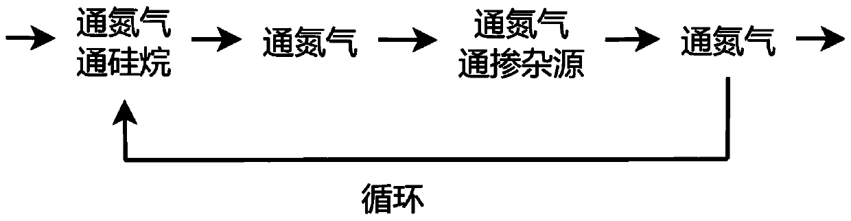
[0069] Take LPCVD doping as an example:

[0070] (1) Prepare 10 polished slices, 5 slices in group A grow a 100nm oxide layer, and 5 slices in group B are cleaned with hydrofluoric acid.

[0071] (2) In the LPCVD furnace cavity, place a quartz boat, and place a silicon wafer of group A and group B at 5 average intervals in the boat from the furnace mouth to the tail of the furnace (positions are respectively numbered 1, 2, 3, 4 , 5).

[0072] (3) Propel the furnace tube, feed oxygen, and carry out the oxidation process at 530° C., and the oxidation time is 10 minutes.

[0073] (4) Evacuate oxygen and check for leaks.

[0074] (5) The temperature is controlled at 580° C., the pressure is 500 mtorr, and the flow rate of nitrogen gas is maintained at 200 sccm, and nitrogen gas is still supplied at 200 sccm when the dopant source gas is supplied.

[0075] (6) silane, phosphine, silane, phosphine are circulated successively, (phosphine is diluted to a volume concentration of 3%)...


PUM


Abstract

The invention provides a process method for carrying out deposition doping on a silicon surface. The process method comprises a cavity capable of accommodating a silicon wafer and allowing silicon tobe subjected to surface deposition doping reaction in the cavity, gas used for deposition doping and/or facilitating deposition doping can be introduced into the cavity. The chamber can be sealed, gascan be introduced into or released from the chamber, temperature control or pressure regulation can be carried out in the chamber, and different or the same gas is introduced into the chamber at intervals in turn in the deposition doping reaction process by the process method in the chamber. According to the process method, the doping concentration is improved, and the uniform distribution of thedoping source is improved.

Description

technical field [0001] The invention relates to the fields of solar photovoltaic and semiconductor manufacturing, and is especially suitable for deposition and doping processes therein. Background technique [0002] In the fields of solar photovoltaic and semiconductor manufacturing, diffusion equipment is mainly used for processes such as boron doping or phosphorus doping, and low-pressure chemical vapor deposition (LPCVD) equipment is often used for silicon oxide, silicon nitride, amorphous silicon, polysilicon, phosphorus-doped amorphous Thin films such as crystalline silicon and boron-doped amorphous silicon are grown; after the temperature and pressure of these conventional diffusion equipment reach the process conditions, the doping source gas, carrier gas, and reaction gas enter the furnace together to participate in the reaction. [0003] In the conventional LPCVD doping process, silane is used as the gas for growing silicon, and phosphine, diborane, etc. are used as...

Claims


Application Information

Patent Timeline
Patent Type & Authority Applications(China)
IPC IPC(8): H01L21/205H01L21/223H01L31/18
CPCH01L21/205H01L21/223H01L31/1876Y02P70/50
Inventor 林佳继庞爱锁刘群张武林依婷
Owner LAPLACE RENEWABLE ENERGY TECH CO LTD
Why Eureka
Try Eureka