Electrostatic discharge protection structure and electrostatic discharge protection circuit

An electrostatic discharge protection and electrostatic discharge technology, applied in the direction of circuits, electrical components, electric solid devices, etc., can solve problems such as weak electrostatic stress tolerance, chip failure, poor electrostatic discharge performance, etc., to improve electrostatic discharge protection ability, fast The effect of discharging electrostatic current and improving area utilization

Active Publication Date: 2020-07-14
SEMICON MFG INT (SHANGHAI) CORP +1
View PDF12 Cites 0 Cited by
  • Summary
  • Abstract
  • Description
  • Claims
  • Application Information

AI Technical Summary

Problems solved by technology

[0004] Power management IC (Integrated Circuit, integrated circuit), driver IC and automatic IC play an important role in daily applications, and high-voltage ESD protection is becoming more and more important for these IC devices, but these high-voltage IC devices are due to their inherent electrostatic stress tolerance Weak resulting in poor ESD robustness
Moreover, when the voltage connected to the input/output pins of the power management IC (integrated circuit), driver IC, and automatic IC is negative, the parasitic diode in the elec...

Method used


Image

  • Electrostatic discharge protection structure and electrostatic discharge protection circuit
  • Electrostatic discharge protection structure and electrostatic discharge protection circuit
  • Electrostatic discharge protection structure and electrostatic discharge protection circuit

Examples


Embodiment Construction

[0033] Currently formed devices still suffer from poor performance. The reasons for the poor performance of the device are analyzed in conjunction with an electrostatic discharge protection structure.

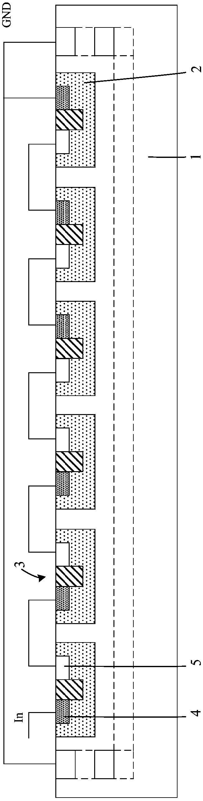
[0034] refer to figure 1 , shows a schematic structural diagram of an electrostatic discharge protection structure.

[0035]The electrostatic discharge protection structure includes: a base 1, a first part (not marked) of the electrostatic discharge protection structure and a second part (not marked) of the electrostatic discharge protection structure are formed in the base 1; the first part of the electrostatic discharge protection structure and the The second part of the electrostatic discharge protection structure includes a plurality of diodes 3 arranged in parallel, and each of the diodes 3 includes a well region 2, and a first doped region 4 and a second doped region located in the well region 2 and isolated from each other. Region 5; the second doped region 5 of the pr...


PUM


Abstract

The invention relates to an electrostatic discharge protection structure and an electrostatic discharge protection circuit, and the structure comprises a substrate which is provided with two drift regions which are arranged in parallel and are isolated from each other; an LDMOS transistor which is located in each drift region and comprises a gate structure, a body region located in the drift region on one side of the gate structure, a source region and a drain region, wherein the source region and the drain region are located on the two sides of the gate structure, and the gate structure stretches across the interface surface of the drift region and the body region; the source regions in the two drift regions are connected; the gate structures are connected with the corresponding source regions; the body region is connected with the peripheral frequency detection circuit, and the peripheral frequency detection circuit pulls up the potential of the body region when detecting an electrostatic discharge signal; and the drain region in one drift region is connected with the electrostatic discharge input end, and the drain region in the other drift region is connected with the groundingend. According to the embodiment of the invention, the problem that the current of the negative voltage signal flows backwards in the electrostatic discharge protection structure when the chip protected by the electrostatic discharge protection structure works normally is avoided, and the electrostatic discharge protection capability of the electrostatic discharge protection structure is improved.

Description

technical field [0001] The embodiments of the present invention relate to the field of electrostatic discharge protection, in particular to an electrostatic discharge protection structure and an electrostatic discharge protection circuit. Background technique [0002] Electrostatic discharge is a common phenomenon in the process of manufacturing, producing, assembling, testing, storing, and transporting semiconductor devices or circuits. The / output pin is passed into the integrated circuit and destroys the internal circuit of the integrated circuit. [0003] In order to solve this problem, it is usually necessary to set up a protection circuit between the internal circuit and the input / output pin. This protection circuit must be activated before the pulse current of electrostatic discharge reaches the internal circuit to quickly eliminate the excessive voltage. Further, damage caused by ESD (Electrostatic Discharge, electrostatic discharge) phenomenon is reduced. [0004]...

Claims


Application Information

Patent Timeline
IPC IPC(8): H01L27/02
CPCH01L27/0266
Inventor 谷欣明程惠娟李宏伟
Owner SEMICON MFG INT (SHANGHAI) CORP
Why Eureka
Try Eureka