Large-size silicon wafer texturing bearing device

A bearing device, large-scale technology, applied in the direction of final product manufacturing, sustainable manufacturing/processing, semiconductor/solid-state device manufacturing, etc., can solve the problem of inability to effectively reduce the pressure basket alarm and machine failure shutdown, increase the weight of the discharge device , Inability to accurately distinguish and other problems, to achieve the effect of good differentiation, high production efficiency, and ensuring stability

Pending Publication Date: 2020-07-17
DONGFANG HUANSHENG PHOTOVOLTAIC (JIANGSU) CO LTD
View PDF1 Cites 1 Cited by
  • Summary
  • Abstract
  • Description
  • Claims
  • Application Information

AI Technical Summary

Problems solved by technology

The patent proposes to use different colors to spray the left and right mounting plates, or to set the same logo as the left and right mounting plates at the place of placement, or to add sensors on the left and right mounting plates, all of which directly or indirectly increase the weight of the discharging device itself. With the prolongation of the texturing time and the erosion of the liquid flow, these additional distinguishing marks will fall off or fail, and cannot be accurately distinguished, resulting in the inability to effectively reduce the probability of pressing basket alarms and machine failures, resulting in low production efficiency and production costs. high

Method used


Image

  • Large-size silicon wafer texturing bearing device
  • Large-size silicon wafer texturing bearing device
  • Large-size silicon wafer texturing bearing device

Examples


Embodiment 1

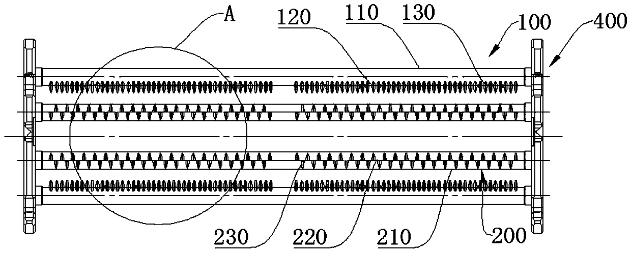
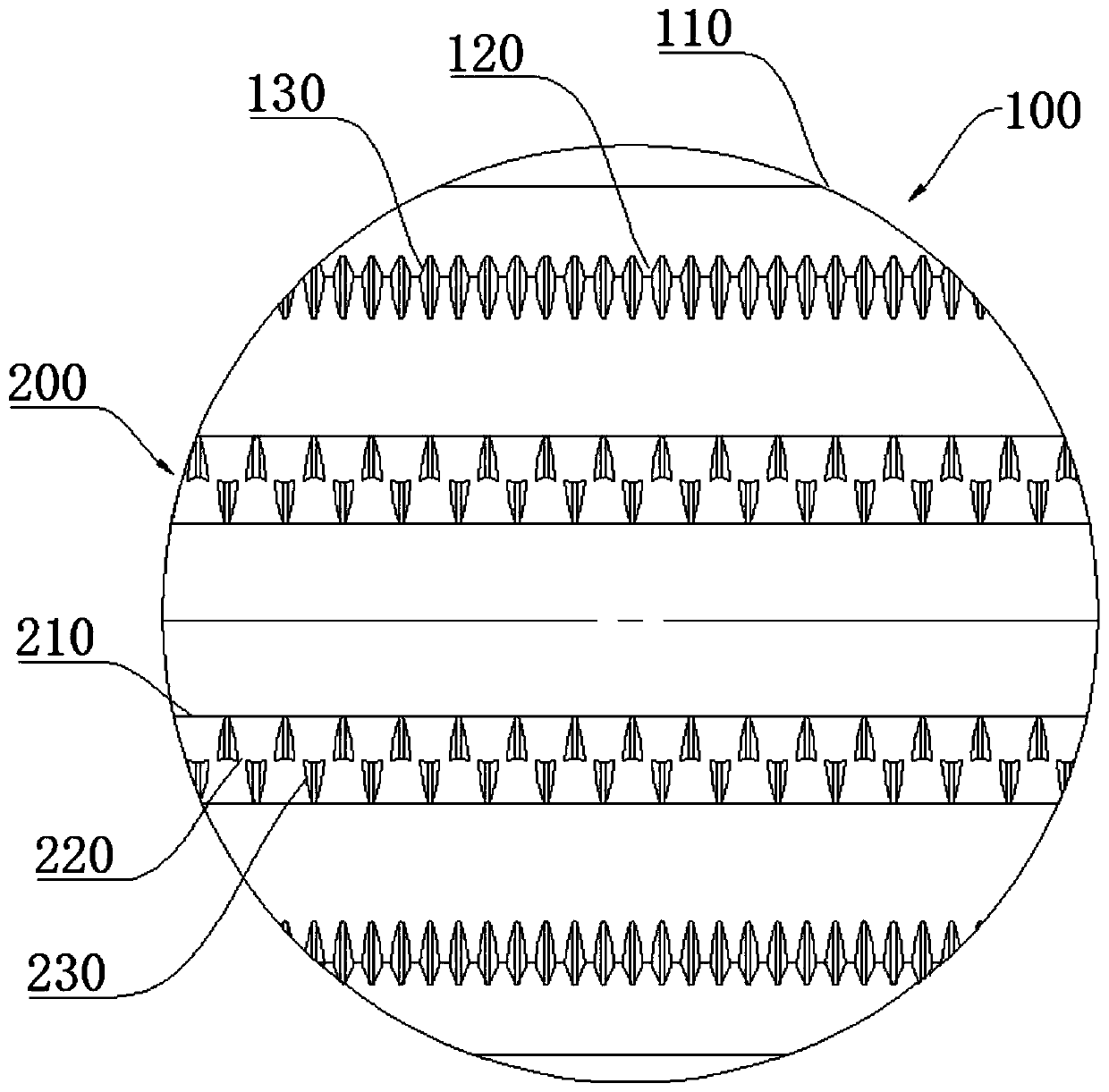
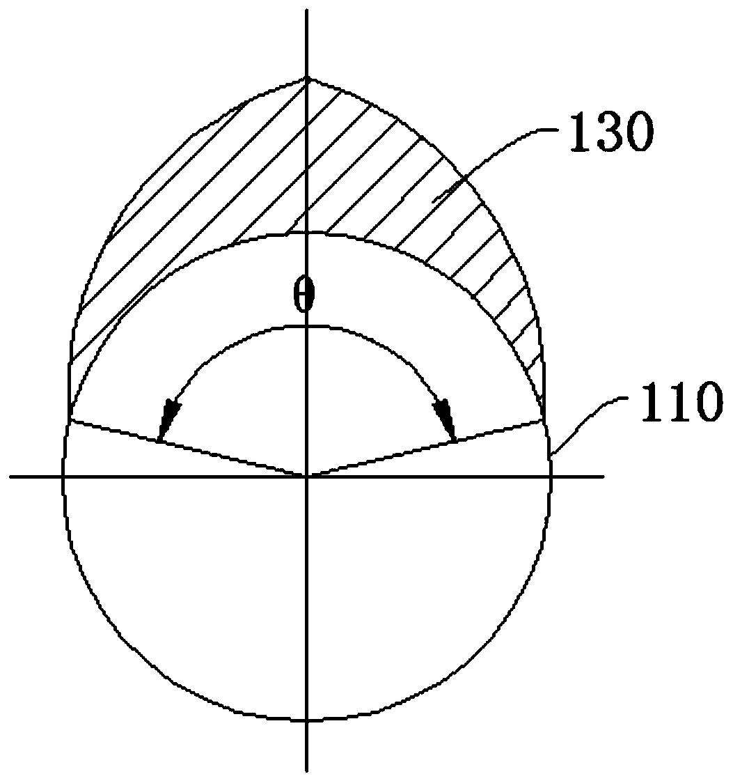
[0042] This embodiment proposes a large-size silicon wafer texturing bearing device, such as figure 1 As shown, it includes a side bar assembly 100, a bottom bar assembly 200, and an end plate assembly 300 placed at both ends of the side bar assembly 100 and the bottom bar assembly 200. The side bar assembly 100 includes several side bars 110, and the bottom bar assembly 200 includes several bottom bars. 210, the end plate assembly 400 includes a left end plate 410 and a right end plate 420, wherein, the outer wall of the side bar 110 is surrounded by a first tooth groove 120, the outer wall of the bottom bar 210 is wound with a second tooth groove 220, the first tooth groove 120 The side bar 110 and the second tooth groove 220 are arranged side by side along the axial length direction of the side bar 110 and the bottom bar 210 respectively, and both are arranged toward the silicon wafer axis direction.

[0043] Due to the large area of ​​the silicon wafer, the vertically plac...

Embodiment 2

[0056] Such as Figure 9 As shown, compared with Embodiment 1, the biggest difference between this embodiment and Embodiment 1 is that the side bar assembly 100 is surrounded by the second tooth groove 220 , and the lower rod assembly 200 is surrounded by the first tooth groove 120 The carrying device set by this structure is formed by the cooperation of the second tooth groove 220 arranged horizontally on the side and the first tooth groove 120 arranged vertically upward on the bottom to form a slot for placing silicon chips, which can also ensure the vertical placement The silicon wafer is clamped stably, which can prevent the silicon wafer from shaking, and at the same time prevent the adjacent silicon wafers from sticking together, so as to not only ensure the uniformity of the texturing of the silicon wafer, but also further reduce the fragmentation rate of the silicon wafer; the smooth design of the first tooth The groove 120 and the second tooth groove 220 allow the tex...

Embodiment 3

[0058] Such as Figure 10 As shown, compared with Embodiment 1, the biggest difference between this embodiment and Embodiment 1 is that the side bar assembly 100 and the lower bar assembly 200 are all wound with first tooth grooves 120. This structure makes the silicon wafer and The contact area of ​​the first tooth groove 120 increases, which in turn can make the placement of the silicon wafer more stable. The stability of the placement of the silicon wafer can further improve the yield of the silicon wafer, and at the same time reduce the probability of the bonding of the silicon wafer, thereby improving the stability of the silicon wafer. Texture-making effect ensures the quality of velvet-making.


PUM


Abstract

The invention provides a large-size silicon wafer texturing bearing device which comprises a side rod assembly and a bottom rod assembly. In the side rod assembly and the bottom rod assembly, a firsttooth groove is formed in one of the side rod assembly and the bottom rod assembly in a wound mode, and a second tooth groove is formed in the other one of the side rod assembly and the bottom rod assembly in a wound mode; or the first tooth groove is formed in the side rod assembly and the bottom rod assembly in a wound mode; or the second tooth groove is formed in the side rod assembly and the bottom rod assembly in a wound mode; the first tooth grooves and the second tooth grooves are formed in the length direction of the side rod assembly and the length direction of the bottom rod assemblyand face the axis of the silicon wafer. According to the bearing device, the silicon wafers can be stably placed without adhesion, no liquid is left, the texturing uniformity of the silicon wafers isensured and the texturing effect is good; meanwhile, the probability of basket pressing alarm and machine fault shutdown can be effectively reduced, normal operation of the machine is guaranteed, theproduction efficiency is high, the universality is wide, the structural design is simple, no relation exists with the size and shape of the silicon wafer and the distinguishing effect is good.

Description

technical field [0001] The invention belongs to the field of solar-grade silicon wafer texturing auxiliary devices, in particular to a large-size silicon wafer texturing bearing device. Background technique [0002] The process of making silicon wafers for solar cells is to place the silicon wafers in the supporting device and use alkali corrosion to remove the mechanically damaged layer on the surface of the silicon wafers and form a pyramid-shaped texture. The carrying device is an important factor to ensure the texturing effect of silicon wafers. With the development of the photovoltaic market, the existing small-sized silicon wafers have small effective areas and low cell conversion rates, which cannot meet the requirements of the market for high power and high conversion rates while reducing production costs for solar cell components. The increase in the size of silicon wafers in tile batteries leads to the increase of the supporting device for placing silicon wafers d...

Claims


Application Information

Patent Timeline
IPC IPC(8): H01L21/687H01L31/18H01L31/0236C30B33/10
CPCC30B33/10H01L21/68771H01L21/68785H01L31/02363H01L31/1804Y02P70/50
Inventor 朱军谈锦彪从海泉苗劲飞马擎天
Owner DONGFANG HUANSHENG PHOTOVOLTAIC (JIANGSU) CO LTD
Why Eureka
Try Eureka