Silicon-on-insulator transverse insulated gate bipolar transistor with low saturation current

A technology of bipolar transistors and silicon-on-insulators, applied in circuits, electrical components, semiconductor devices, etc., can solve the problems of reduced injection efficiency, complex drive circuits, and increased conduction voltage drop, and achieve increased base drive current. The effect of large, increased number of holes, and large linear current

Active Publication Date: 2020-07-17
SOUTHEAST UNIV
View PDF6 Cites 1 Cited by
  • Summary
  • Abstract
  • Description
  • Claims
  • Application Information

AI Technical Summary

Problems solved by technology

However, both devices require two gates, and during the turn-off process and the short-circuit switching process, the time phase of the switching signals of the two gates needs to be precisely controlled to obtain ideal performance, which makes the driving circuit variable. complicated
For example, a device with an additional trench added to the anode, this type of structure can effectively shorten the turn-off time and reduce the turn-off loss, but because the anode area is reduced, the injection efficiency is reduced, thereby increasing the conduction voltage drop, making the conduction The trade-off relationship between on-voltage drop and off loss becomes worse

Method used


Image

  • Silicon-on-insulator transverse insulated gate bipolar transistor with low saturation current
  • Silicon-on-insulator transverse insulated gate bipolar transistor with low saturation current
  • Silicon-on-insulator transverse insulated gate bipolar transistor with low saturation current

Examples


Embodiment Construction

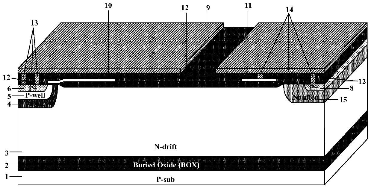
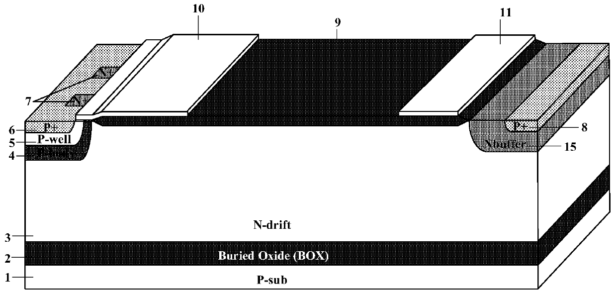
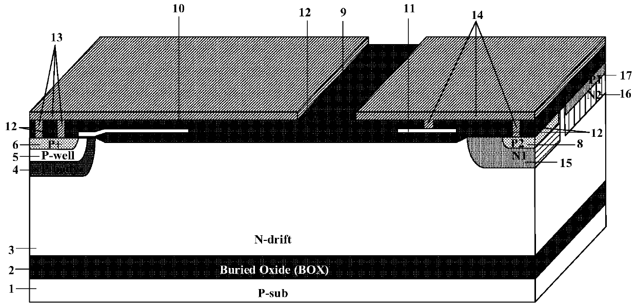
[0022] Combine below image 3 and Figure 4 , the present invention is described in detail, a silicon-on-insulator lateral insulated gate bipolar transistor with low saturation current, comprising: a P-type substrate 1, a buried oxide layer 2 is arranged above the P-type substrate 1, and a buried oxide layer is formed on the buried oxide layer An N-type drift region 3 is provided above 2, and a P-type body region 4, a field oxygen layer 9 and a collector region are arranged below the emitter side of the upper surface in the N-type drift region 3, and the field oxygen layer 9 is located in the P-type body Between the region 4 and the collector region, a connected P well 5 is provided in the P-type body region 4, a P-type emitter region 6 is arranged in the P-type body region 5, and an N-type emitter region is arranged on the P-type emitter region 6. The emitter region 7 is provided with an oxide layer 12 above the P-type body region 4, the P well 5, the P-type emitter region 6...


PUM


Abstract

The invention discloses a silicon-on-insulator transverse insulated gate bipolar transistor with low saturation current. The According to the semiconductor is provided with:, a semiconductor substrate; wherein a buried oxide layer is arranged on the a P-type substrate; an N-type drift region is arranged above on the buried oxide layer; , wherein a P-type body region, a field oxide layer and a collector region are arranged on the N-type drift regionsubstrate; connected P traps are arranged in the P-type body region; a P-type emitter region is arranged in the P traps; an N-type emitter region isarranged on the P-type emitter region; an oxide layer is arranged above on the P-type body region, the P traps, the P-type emitter region, the field oxide layer and the collector region; a polysilicon gate is arranged between the field oxide layer and the oxide layer and extends to the upper part of the P traps; a gate oxide layer is arranged among the P traps, the P-type body region and the polysilicon gate,; wherein the collector region comprises a heavily-doped N-type collector region and a lightly-doped N-type collector region which are arranged in the N-type drift region and isolated bythe N-type drift region, a lightly-doped P-type collector region is arranged in the heavily-doped N-type collector region, and a heavily-doped P-type collector region is arranged in the lightly-dopedN-type collector region.

Description

technical field [0001] The invention mainly relates to the technical field of power semiconductor devices, and is a silicon-on-insulator lateral insulated gate bipolar transistor with low saturation current, which is suitable for many integrated power chips such as switching power supplies and household appliances. Background technique [0002] The insulated gate bipolar transistor is a composite semiconductor power device that combines the MOS structure and the bipolar crystal structure, and it better combines the advantages of the MOS transistor and the bipolar transistor. It is widely used in the fields of switching power supply, household appliances, smart grid and traffic transmission. Among them, the silicon-on-insulator lateral insulated gate bipolar transistor (SOI-LateralInsulated Gate Bipolar Transistor, SOI-LIGBT) is a typical structure based on the SOI process, which has the advantages of easy integration, high withstand voltage, strong drive current capability, ...

Claims


Application Information

Patent Timeline
Patent Type & Authority Applications(China)
IPC IPC(8): H01L29/739H01L29/06H01L29/08
CPCH01L29/7394H01L29/0619H01L29/0821
Inventor 张龙龚金丽祝靖杨兰兰孙伟锋时龙兴
Owner SOUTHEAST UNIV
Why Eureka
Try Eureka