Silicon carbide crystal growth device and preparation method thereof

A growth device, silicon carbide technology, applied in the directions of crystal growth, single crystal growth, single crystal growth, etc., can solve the problems of resource waste, inclusion defects, affecting the quality of silicon carbide crystals, etc., to achieve high purity and high utilization rate. Effect

Active Publication Date: 2020-07-28
金华博蓝特新材料有限公司
View PDF4 Cites 5 Cited by
  • Summary
  • Abstract
  • Description
  • Claims
  • Application Information

AI Technical Summary

Problems solved by technology

As the growth progresses, the surface of the crystal will be wrapped by carbon particles, forming inclusion defects, affecting the quality of silicon carbide crystals, and the raw material utilization rate in the whole process is not high, and there is a waste of resources

Method used


Image

  • Silicon carbide crystal growth device and preparation method thereof
  • Silicon carbide crystal growth device and preparation method thereof
  • Silicon carbide crystal growth device and preparation method thereof

Examples


Embodiment Construction

[0023] Exemplary embodiments of the present disclosure will be described in more detail below with reference to the accompanying drawings. Although exemplary embodiments of the present disclosure are shown in the drawings, it should be understood that the present disclosure may be embodied in various forms and should not be limited by the embodiments set forth herein. Rather, these embodiments are provided for more thorough understanding of the present disclosure and to fully convey the scope of the present disclosure to those skilled in the art.

[0024] In order to achieve the desired function, the present invention provides a silicon carbide crystal growth device and a preparation method thereof.

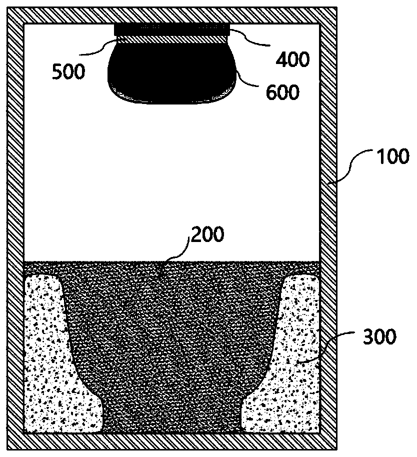
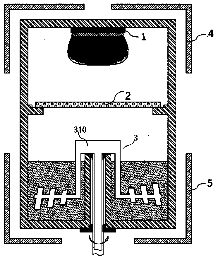
[0025] The traditional physical vapor transport (PVT) method to grow silicon carbide crystals is realized by specific preparation devices, such as figure 1 As shown, the preparation device includes a crucible 100. After heating the crucible 100, the gaseous matter evaporated fro...


PUM

PropertyMeasurementUnit
electrical resistivityaaaaaaaaaa

Abstract

The invention relates to a silicon carbide crystal growth device and a preparation method thereof. The growth device comprises a crucible, a seed crystal seat provided with seed crystals, a graphite filter plate, a stirring device, a top heater and a bottom heater; the seed crystal seat, the graphite filter plate and the stirring device are all located in the crucible, wherein the seed crystal seat is fixed at the top of the crucible; the seed crystals are arranged downwards, the graphite filter plate is located in the middle of the crucible and divides the crucible into an upper half part anda lower half part, the stirring device is located at the lower half part, and the top heater and the bottom heater are both arranged outside the crucible. The preparation method comprises the step ofgrowing the silicon carbide crystal by using the growth device. The silicon carbide prepared by the growth device and the preparation method thereof has the advantages of few impurities, high purity,no inclusion defect, high raw material utilization rate and cost saving.

Description

technical field [0001] The invention belongs to the field of crystal growth, in particular to a silicon carbide crystal growth device and a preparation method thereof. Background technique [0002] As a representative of the third-generation semiconductor material, silicon carbide has the characteristics of energy bandwidth, high thermal conductivity, high saturation drift velocity of electrons, high critical breakdown electric field, low dielectric constant, and good chemical stability. It is an ideal material for high-frequency, high-power, radiation-resistant, short-wavelength light-emitting and photoelectric integration components. It has broad application prospects in high-frequency, high-power, high-temperature-resistant, radiation-resistant semiconductor components and ultraviolet detectors. . [0003] At present, the physical vapor transport (PVT) method is the main growth technology for the production of silicon carbide single crystals. The gas phase substances pro...

Claims


Application Information

Patent Timeline
Patent Type & Authority Applications(China)
IPC IPC(8): C30B23/00C30B29/36
CPCC30B23/00C30B23/002C30B29/36
Inventor 徐良杨新鹏蓝文安刘建哲余雅俊夏建白李京波郭炜叶继春
Owner 金华博蓝特新材料有限公司
Why Eureka
Try Eureka