

Passivated contact N type back junction solar cell and preparation method thereof
A solar cell, N-type technology, used in circuits, photovoltaic power generation, electrical components, etc., can solve problems such as difficulty, low short-circuit current of solar cells, and large light absorption coefficient
- Summary
- Abstract
- Description
- Claims
- Application Information
AI Technical Summary
Problems solved by technology
Method used
Image

Examples
Embodiment Construction
[0034] In order to make the technical means, creative features, goals and effects achieved by the present invention easy to understand, the present invention will be further described below in conjunction with specific illustrations.
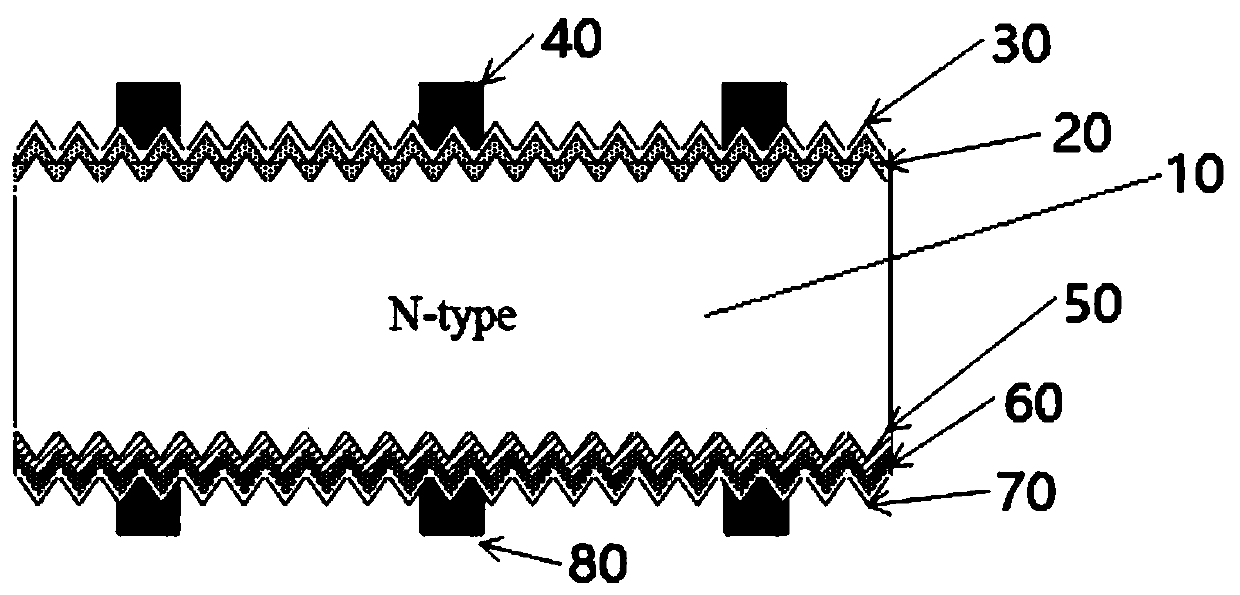
[0035] according to Figure 1 to Figure 9 As shown, the N-type back-junction solar cell with passivation contact provided by the present invention includes an N-type crystalline silicon wafer 10, and the front surface of the N-type crystalline silicon wafer 10 is sequentially provided with N+ front surface field doped regions 20 from inside to outside. , front surface passivation anti-reflection layer 30 and metal contact electrode 40, the back surface of N-type crystalline silicon chip 10 is provided with tunnel oxide layer 50, P+ doped polysilicon region 60, back surface passivation anti-reflection Layer 70 and metal contact electrode 80; tunnel oxide layer 50, P+ doped polysilicon region 60 and back surface passivation anti-reflection layer 7...
PUM
| Property | Measurement | Unit |
|---|---|---|
| Etching depth | aaaaa | aaaaa |
| Thickness | aaaaa | aaaaa |
| Thickness | aaaaa | aaaaa |
Abstract
Description
Claims
Application Information