Preparation method of rewiring layer and semiconductor structure

A technology for rewiring layers and semiconductors, applied in the fields of semiconductor devices, semiconductor/solid-state device manufacturing, semiconductor/solid-state device components, etc., can solve the problems of high cost, long time, and complex RDL process, avoid grooves, improve Flatness, the effect of reducing process risk

Pending Publication Date: 2020-08-04
SJ SEMICON JIANGYIN CORP
View PDF0 Cites 0 Cited by
  • Summary
  • Abstract
  • Description
  • Claims
  • Application Information

AI Technical Summary

Problems solved by technology

[0007] In view of the shortcomings of the prior art described above, the object of the present invention is to provide a method for preparing a rewiring layer and a semiconductor structure, which are used to solve the problems of complex, time-consuming, and high-cost preparation of RDL in the prior art, and The above-mentioned series of process problems caused by the deep grooves in the prepared RDL

Method used


Image

  • Preparation method of rewiring layer and semiconductor structure
  • Preparation method of rewiring layer and semiconductor structure
  • Preparation method of rewiring layer and semiconductor structure

Examples


Embodiment 1

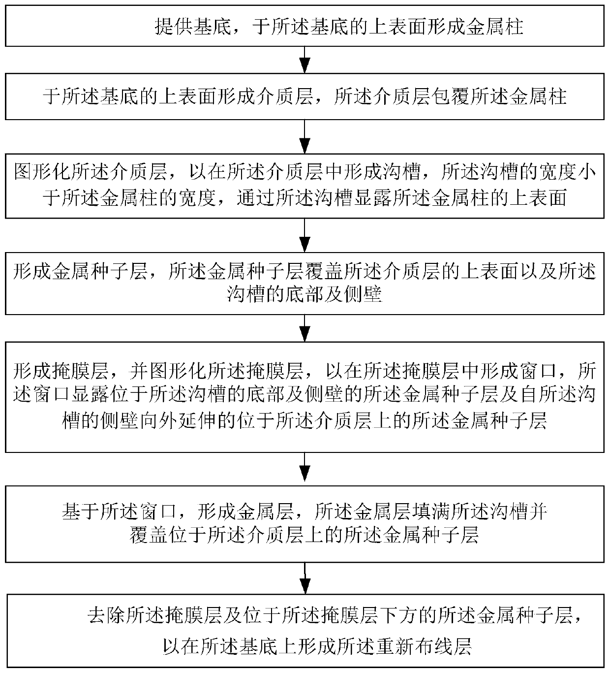
[0059] like figure 1 , this embodiment provides a method for preparing a rewiring layer, comprising the following steps:

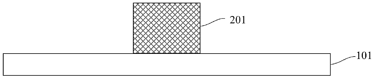
[0060] providing a base, and forming metal pillars on the upper surface of the base;

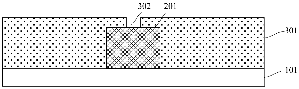
[0061] forming a dielectric layer on the upper surface of the substrate, the dielectric layer covering the metal pillar;

[0062] patterning the dielectric layer to form a groove in the dielectric layer, the width of the groove is smaller than the width of the metal pillar, and the upper surface of the metal pillar is exposed through the groove;

[0063] forming a metal seed layer, the metal seed layer covering the upper surface of the dielectric layer and the bottom and sidewalls of the trench;

[0064] forming a mask layer, and patterning the mask layer to form windows in the mask layer that expose the metal seed layer at the bottom and sidewalls of the trench and from the trench the metal seed layer on the dielectric layer with the sidewalls of the groove extending...

Embodiment 2

[0092] like Figure 7a , this embodiment also provides a semiconductor structure, the semiconductor structure includes: a base 101 and a rewiring layer, and the rewiring layer is located on the upper surface of the base 101 . Wherein, the rewiring layer includes: metal pillars 201, the metal pillars 201 are located on the upper surface of the substrate 101; a dielectric layer 301, the dielectric layer 301 is located on the upper surface of the substrate 101, and the dielectric layer 301 Covering the metal pillar 201, and the dielectric layer 301 includes a groove 302, the width of the groove 302 is smaller than the width of the metal pillar 201, and the upper surface of the metal pillar 201 is exposed through the groove 302. surface; a metal seed layer 401, the metal seed layer 401 covers the upper surface of the dielectric layer 301 and the bottom and sidewalls of the trench 302; a metal layer, the metal layer fills the trench 302 and covers The metal seed layer 401 located ...


PUM

PropertyMeasurementUnit
Thicknessaaaaaaaaaa
Thicknessaaaaaaaaaa
Widthaaaaaaaaaa

Abstract

The invention provides a preparation method of a rewiring layer and a semiconductor structure. The semiconductor structure comprises a substrate and the rewiring layer located on the upper surface ofthe substrate. The rewiring layer comprises a metal column; a dielectric layer, wherein the dielectric layer wraps the metal column, and the dielectric layer comprises a trench, the width of the trench being smaller than that of the metal column, and the upper surface of the metal column being exposed through the trench; a metal seed layer, which covers the upper surface of the dielectric layer and the bottom and the side wall of the trench; and a metal layer which fills the trench and covers the metal seed layer on the dielectric layer. According to the invention, the depth-to-width ratio oftrench filling in the dielectric layer is reduced by manufacturing the early-stage metal columns, and then the metal layer is manufactured, so that the flatness of the rewiring layer can be improved,grooves are prevented from being generated in the formed rewiring layer, the subsequent manufacturing process is facilitated, the process risk of multilayer stacking is reduced, and the process difficulty and cost are reduced.

Description

technical field [0001] The invention belongs to the field of semiconductor manufacturing, and relates to a preparation method of a rewiring layer and a semiconductor structure. Background technique [0002] With the increasingly powerful functions, higher performance and integration of integrated circuits, and the emergence of new integrated circuits, packaging technology plays an increasingly important role in integrated circuit products, and in the value of the entire electronic system The proportion is increasing. At the same time, as the feature size of integrated circuits reaches the nanometer level, transistors are developing towards higher density and higher clock frequency, and packaging is also developing towards higher density. [0003] Due to the advantages of miniaturization, low cost, high integration, better performance and higher energy efficiency, wafer-level packaging (WLP) technology has become an important part of electronic equipment such as demanding mo...

Claims


Application Information

Patent Timeline
IPC IPC(8): H01L21/60H01L23/48
CPCH01L23/481H01L24/02H01L2224/0231H01L2224/02331H01L2224/02372
Inventor 周祖源赵强陈彦亨吴政达林正忠
Owner SJ SEMICON JIANGYIN CORP
Why Eureka
Try Eureka