
Fabrication method of arrayed optical waveguide flexible tactile sensor

A tactile sensor and optical waveguide technology, applied in the direction of optical waveguide light guide, measurement of the change force of the optical properties of the material when it is stressed, instruments, etc., can solve the large-scale array resistance of tactile sensors, fewer application scenarios, Difficulty in packaging and other issues, to achieve the effect of automatic detection, simple process, and convenient integration

Active Publication Date: 2021-04-27
TSINGHUA UNIV
View PDF6 Cites 0 Cited by
  • Summary
  • Abstract
  • Description
  • Claims
  • Application Information

AI Technical Summary

Problems solved by technology

The electromagnetic flexible tactile sensor solves the problem of removing the tow cable from the sensor, but at the same time introduces the need for a professional detection environment, which reduces the ease of integration and fewer application scenarios
Liquid metal can maintain followability with the soft substrate and reflect tactile information through the change of resistance value, but it has the disadvantages of high packaging difficulty and easy leakage, and the static working zero point may change continuously with deformation
At the same time, an unavoidable problem for different tactile sensors is that as the sensing area continues to increase and the number of sensitive nodes increases, the amount of data to be processed also increases geometrically, which poses a great challenge to the processing circuit. The large-scale array of sensors brings resistance

Method used


Image

  • Fabrication method of arrayed optical waveguide flexible tactile sensor
  • Fabrication method of arrayed optical waveguide flexible tactile sensor
  • Fabrication method of arrayed optical waveguide flexible tactile sensor

Examples


Embodiment 1

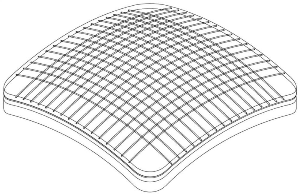
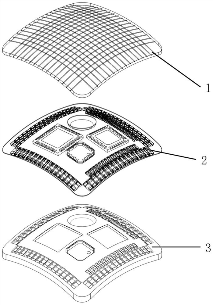
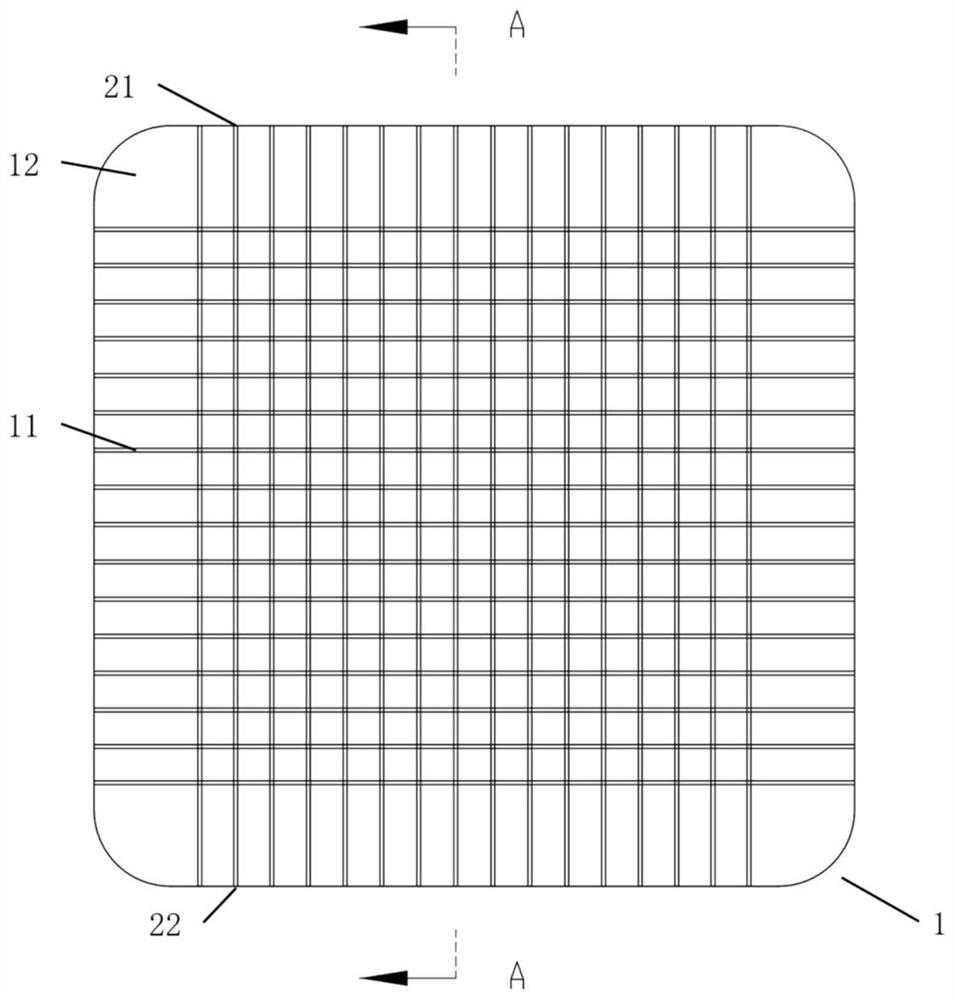
[0047] like figure 1 , figure 2 As shown, the arrayed optical waveguide flexible tactile sensor includes a flexible optical waveguide tactile sensitive layer 1 , a flexible circuit layer 2 , and a flexible substrate layer 3 distributed in layers from top to bottom. The flexible optical waveguide tactile sensitive layer 1 includes several optical waveguide inner cores 11 and an optical waveguide cladding 12 integrally covering the optical waveguide inner cores 11 . Wherein the optical waveguide inner cores 11 are distributed in an array. The flexible circuit layer 2 includes a light-emitting power supply terminal and an optical signal receiving and processing terminal. The flexible substrate layer 3 is made of a flexible material with an adaptable shape, which plays the role of protection and auxiliary fixation. The flexible optical waveguide tactile sensitive layer 1, the flexible circuit layer 2 and the flexible substrate layer 3 are bonded and packaged by silicone rubber...

Embodiment 2

[0078] Such as Figure 7 to Figure 9(b) As shown, one of the differences between this embodiment and Embodiment 1 is that the surface curvatures of the flexible optical waveguide tactile sensitive layer 1, the flexible circuit layer 2, and the flexible substrate 3 are different, and the three-layer structures are all planes; the second difference lies in the flexible The number of optical waveguide inner cores in the optical waveguide tactile sensitive layer is different and is eight. The difference between the technical effect produced by this embodiment and the first embodiment is that it is more suitable for the working environment where the sensitive area is a plane.

[0079] In addition, other contents of this embodiment, including the internal structure and function of the flexible optical waveguide tactile sensitive layer 1, the flexible circuit layer 2, and the flexible substrate 3, and the working principle and preparation method of the tactile sensor, are all consist...

Embodiment 3

[0081] As shown in FIG. 10( a ) and FIG. 10( b ), the difference between this embodiment and the first embodiment is that the optical waveguide inner core 11 in the flexible optical waveguide tactile sensitive layer 1 is distributed in a single layer. The difference between the technical effect produced by this embodiment and the first embodiment is that the number of inner cores of the optical waveguide in the tactile sensitive layer of the flexible optical waveguide is reduced, the difficulty of preparation is reduced, and it is more suitable for detecting whether a collision has occurred on the sensitive surface, rather than extracting Richer tactile information.

[0082] In addition, other contents of this embodiment, including the internal structure and function of the flexible optical waveguide tactile sensitive layer 1, the flexible circuit layer 2, and the flexible substrate 3, and the working principle and preparation method of the tactile sensor, are all consistent wi...


PUM


Abstract

The invention discloses a preparation method of an arrayed optical waveguide flexible tactile sensor. The tactile sensor includes a flexible optical waveguide tactile sensitive layer, a flexible circuit layer and a flexible substrate layer glued in sequence. The flexible optical waveguide tactile sensitive layer includes several optical waveguide inner cores distributed in an array, and an optical waveguide cladding integrally covering the optical waveguide inner core. The flexible circuit layer includes a light-emitting power supply end and an optical signal receiving and processing end. The light-emitting power supply end generates an optical signal, and the optical signal is transmitted to the optical signal receiving and processing end through the optical waveguide, and is converted into an electrical signal by the optical signal receiving and processing end, and sent as a wireless signal. go out. The flexible substrate layer is made of flexible material, which plays the role of protection and auxiliary fixation. The tactile sensor of the invention can be used for the collection and processing of tactile information, and has the advantages of high flexibility, high sensitivity, high spatial resolution density and the like. The structure is simple, the power consumption is low, and it is convenient to integrate with the environment to be tested, and it has the advantage of low data cost when the sensing area increases.

Description

technical field [0001] The invention belongs to the technical field of flexible tactile sensors and soft robots, in particular to an arrayed optical waveguide flexible tactile sensor and its preparation method and application. Background technique [0002] Tactile sensors are usually used to collect tactile information such as force, shape, and pressure, and have a wide range of applications in robotics, wearable devices, virtual reality, intelligent prosthetics, and human-computer interaction. Traditional tactile sensors are often prepared by silicon-based semiconductor technology or MEMS (Microelectro Mechanical Systems, microelectromechanical systems) technology, mostly rigid, and are arranged in joints or other positions of interest to measure or calculate the tactile sensation during the interaction process. information. However, compared with the biological skin of the touch, the information collected in this way is often discrete and single-point, and the tactile inf...

Claims


Application Information

Patent Timeline
Patent Type & Authority Patents(China)
IPC IPC(8): G02B6/10G01L1/24G01N21/84G01N21/88
CPCG01L1/24G01N21/84G01N21/88G02B6/10
Inventor 赵慧婵周婧祎刘辛军乔飞
Owner TSINGHUA UNIV
Learn More