Stealth destroy-resistant shielding material and preparation method thereof
A technology of shielding materials and wave-absorbing materials, which is applied in the field of stealth and anti-destruction shielding materials and its preparation, can solve the problems of large overall thickness and large surface density, and achieve the effect of solving low surface density
- Summary
- Abstract
- Description
- Claims
- Application Information
AI Technical Summary
Problems solved by technology
Method used
Image
Examples
Embodiment 1
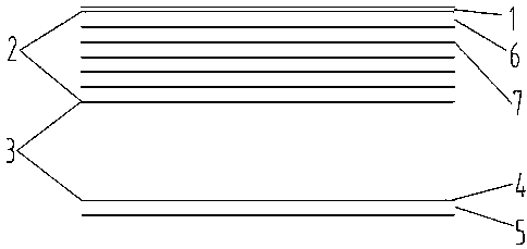
[0039] A stealth and anti-destroy shielding material, its structure schematic diagram is as follows figure 1 As shown, it is composed of a skin layer 1, a wave-absorbing foam layer 2, an indestructible layer 3, an electromagnetic shielding enhancement layer 4 and a reflective layer 5, wherein the wave-absorbing foam layer 2 is covered with a periodic hollow structure patterned absorbing layer. Wave material 7 compounded:
[0040] 1) Each layer is composited with E51 epoxy resin;
[0041] 2) The skin layer is made of quartz fiber with a thickness of 0.4mm and a relative dielectric constant of 2;
[0042]3) The foam of the wave-absorbing foam layer is PVC, a total of six layers, the first layer is 2.5mm, the second layer is 3.98mm, the third layer is 2.38mm, the fourth layer is 3.97mm, the fifth layer is 1.79mm, and the sixth layer is 4.79mm ;
[0043] 4) The anti-destruction layer is a single-layer bullet-proof board, selected from high-density polyethylene bullet-proof boar...
Embodiment 2
[0055] A stealth and anti-destroy shielding material, its structure schematic diagram is as follows figure 1 As shown, it is composed of a skin layer 1, a wave-absorbing foam layer 2, an indestructible layer 3, an electromagnetic shielding enhancement layer 4 and a reflective layer 5, wherein the wave-absorbing foam layer 2 is covered with a periodic hollow structure patterned absorbing layer. Wave material 7 compounded:
[0056] 1) Each layer is composited with 901 vinyl resin;
[0057] 2) The skin layer is made of glass fiber with a thickness of 0.2mm and a relative dielectric constant of 2.5;
[0058] 3) The foam of the wave-absorbing foam layer is PU, a total of six layers, the first layer is 1.5mm, the second layer is 2.36mm, the third layer is 3.66mm, the fourth layer is 2.98mm, the fifth layer is 0.75mm, and the sixth layer is 2.75mm ;
[0059] 4) The anti-destruction layer is a single-layer bullet-proof board, selected from high-density polyethylene bullet-proof boa...
Embodiment 3
[0071] A stealth and anti-destroy shielding material, its structure schematic diagram is as follows figure 1 As shown, it is composed of a skin layer 1, a wave-absorbing foam layer 2, an indestructible layer 3, an electromagnetic shielding enhancement layer 4 and a reflective layer 5, wherein the wave-absorbing foam layer 2 is covered with a periodic hollow structure patterned absorbing layer. Wave material 7 compounded:
[0072] 1) Each layer is composited with 901 vinyl resin;
[0073] 2) The skin layer is made of aramid fiber with a thickness of 0.5mm and a relative dielectric constant of 5;
[0074] 3) The foam of the wave-absorbing foam layer is PMI, a total of six layers, the first layer is 1.5mm, the second layer is 2.36mm, the third layer is 4.55mm, the fourth layer is 2.98mm, the fifth layer is 0.50mm, and the sixth layer is 5.00mm ;
[0075] 4) The anti-destruction layer is a single-layer bullet-proof board, selected from high-density polyethylene bullet-proof boa...
PUM
| Property | Measurement | Unit |
|---|---|---|
| Thickness | aaaaa | aaaaa |
| Thickness | aaaaa | aaaaa |
| Thickness | aaaaa | aaaaa |
Abstract
Description
Claims
Application Information

