
Preparation method of silicon drift detector

A silicon drift detector and silicon substrate technology, which is applied in semiconductor devices, final product manufacturing, sustainable manufacturing/processing, etc., can solve the difficulty of ultra-shallow junction preparation process, the surface damage of silicon substrate, and the inability to completely repair it, etc. question

Active Publication Date: 2022-05-03
INST OF MICROELECTRONICS CHINESE ACAD OF SCI
View PDF0 Cites 0 Cited by
  • Summary
  • Abstract
  • Description
  • Claims
  • Application Information

AI Technical Summary

Problems solved by technology

Although the method of ion implantation can control the concentration of dopants and the doping depth of formation more accurately, it also has corresponding shortcomings: (1) During the ion implantation process, high-energy ions will cause damage to the surface of the silicon substrate; The damage needs to be repaired by high-temperature annealing process, but it cannot be completely repaired; (2) After boron ion implantation, a higher temperature is required for activation, and the activation temperature is about 1000 ° C; but the high-temperature activation process will cause the quality of the silicon substrate to deteriorate; (3) The minimum junction depth formed by ion implantation is 40nm, which is greater than the depth process requirements of ultra-shallow junctions currently required. This depth makes the preparation process of ultra-shallow junctions difficult; Conducive to the detection of low-energy X-rays: (4) During the activation process after ion implantation, there is a phenomenon of lateral expansion of dopant atoms, which increases the image size of the drift ring of the silicon drift detector

Method used


Image

  • Preparation method of silicon drift detector
  • Preparation method of silicon drift detector

Examples


Embodiment Construction

[0037] Preferred embodiments of the present invention will be described in detail below in conjunction with the accompanying drawings, wherein the accompanying drawings constitute a part of the application and together with the embodiments of the present invention are used to explain the principle of the present invention and are not intended to limit the scope of the present invention.

[0038] figure 1 is a schematic diagram of the junction cross-section of the silicon drift detector provided in the embodiment. Such as figure 1 As shown, the silicon drift detector provided in this embodiment includes an N-type doped silicon substrate 11 , passivation films 12 and functional regions disposed on both surfaces of the silicon substrate 11 .

[0039] The functional area includes an N-type heavily doped collector electrode 13, a P-type heavily doped drift ring 14, a P-type heavily doped guard ring 15, and an N-type heavily doped grounding ring 16 arranged on one side of the silic...


PUM

PropertyMeasurementUnit
thicknessaaaaaaaaaa
thicknessaaaaaaaaaa
thicknessaaaaaaaaaa

Abstract

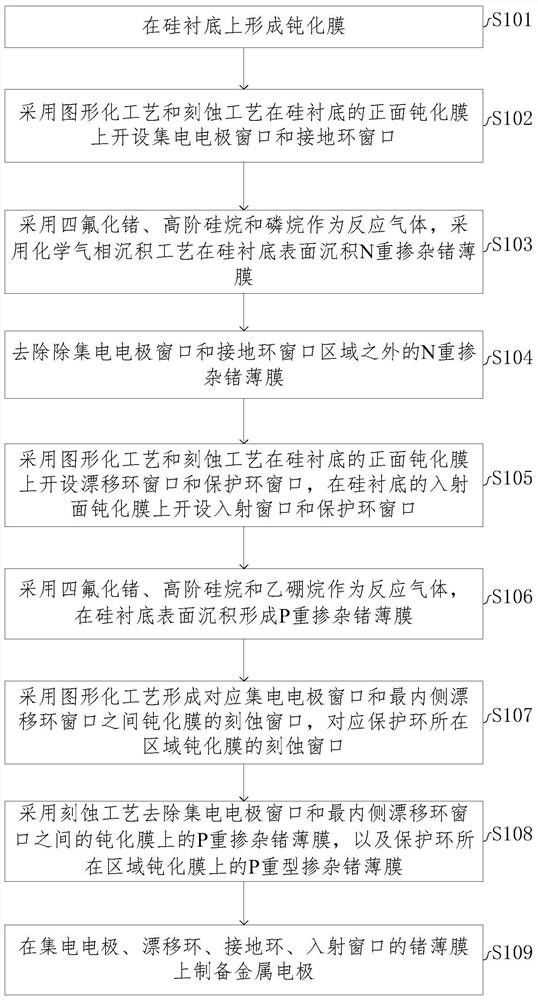
This specification provides a method for preparing a silicon drift detector, including a deposition step; The heavily doped germanium thin film is deposited on the silicon substrate of the film, so that the heavily doped germanium thin film forms a functional area in the corresponding area of ​​the silicon substrate. Because high-order silane can be activated at a lower temperature to react with germanium tetrafluoride, a low-temperature process can be used in the formation of germanium thin films, and the low-temperature process can avoid the high temperature in the diffusion process and discrete implantation process on the silicon substrate. The damage is beneficial to obtain a higher bulk lifetime and improve the energy resolution of the silicon drift detector.

Description

technical field [0001] This specification relates to the technical field of semiconductor devices, in particular to a method for preparing a silicon drift detector. Background technique [0002] Drift detectors are semiconductor detectors used to detect high-energy rays (generally, drift detectors are silicon-based detectors). When the drift detector is working, the drift ring makes the substrate in a completely depleted state, and the majority carriers formed on the substrate by high-energy rays passing through the incident window drift to the collector electrode along the direction of the device surface and are collected. [0003] In the current manufacturing process of silicon drift detectors, ion implantation is used to achieve doping of corresponding functional regions. Although the method of ion implantation can control the concentration of dopants and the doping depth of formation more accurately, it also has corresponding shortcomings: (1) During the ion implantatio...

Claims


Application Information

Patent Timeline
Patent Type & Authority Patents(China)
IPC IPC(8): H01L31/18H01L31/118H01L31/028
CPCH01L31/1808H01L31/1185H01L31/028Y02P70/50
Inventor 陶科贾锐姜帅刘新宇金智张立军王冠鹰欧阳晓平
Owner INST OF MICROELECTRONICS CHINESE ACAD OF SCI
Learn More