Device and method for automatically powdering silicon wafer

A silicon wafer, automatic technology, applied in the direction of electrical components, electrical solid devices, semiconductor/solid device manufacturing, etc., can solve the problems of difficult control of photolithography process and complicated process, and achieve low requirements on the surface of silicon wafers, simple process, non-scratch effect

Pending Publication Date: 2020-08-21
捷捷半导体有限公司
View PDF0 Cites 1 Cited by
  • Summary
  • Abstract
  • Description
  • Claims
  • Application Information

AI Technical Summary

Problems solved by technology

However, the process of this method is complicated, and the photolithography process is not easy to control

Method used


Image

  • Device and method for automatically powdering silicon wafer
  • Device and method for automatically powdering silicon wafer
  • Device and method for automatically powdering silicon wafer

Examples


Embodiment 1

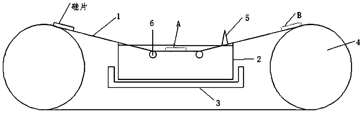
[0036] This embodiment provides a device for automatic powdering of silicon wafers, which has the following functions: figure 1 With the structure shown, the device includes: transmission equipment, powder scraper 5, and powder feeding equipment.

[0037] Wherein, the powdering equipment is used for coating the glass paste on the silicon wafer, and the powdering equipment includes an ultrasonic device 3 and a storage tank 2, the storage tank 2 is used for containing the glass paste, and the ultrasonic device 3 is used for ultrasonically treating the materials in the storage tank, Remove the air bubbles in the groove of the silicon wafer, and fill the uniform glass paste into the groove of the silicon wafer. The storage tank 2 can be arranged inside the ultrasonic device 3 , and the storage tank 2 is arranged between two rotating wheels 4 . Two pulleys 6 are arranged inside the storage tank 2, and the pulleys 6 are used to make the conveyor belt 1 pass through the glass paste....

Embodiment 2

[0051] This example provides the use of figure 1 The automatic powder feeding method that the shown device completes specifically includes:

[0052] By photolithography, the area that does not need to be grooved is protected;

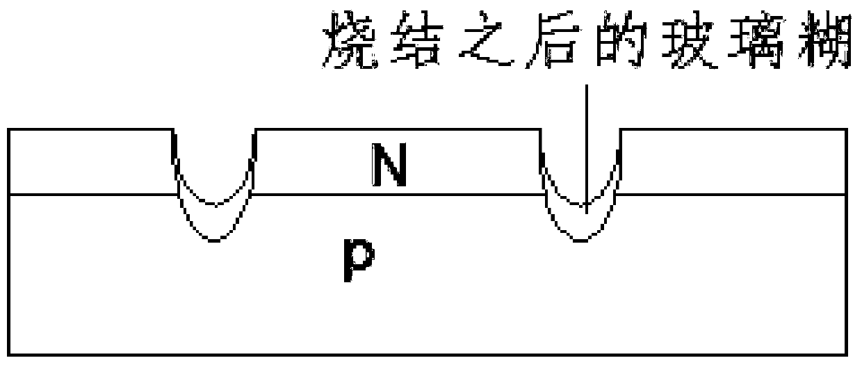
[0053] The PN junction of the silicon wafer is dug out by acid rot to form a clean PN junction section, and the acid solution is HF:HNO 3 =1:3;

[0054] Load silicon wafers to figure 1 On the device shown, it is required that the grooves produced by corrosion form an angle of 75° with the belt running track, and the silicon wafers are fed into the glass paste (the composition of the glass paste is glass powder and butyl with a mass ratio of 3:1) through the conveyor belt. Carbitol storage tank, and at a speed of 3mm / sec, the running distance of the silicon wafer in the glass paste is 12cm, and the air bubbles in the silicon wafer groove are removed by ultrasonic waves, and the glass paste is evenly filled into the silicon wafer groove Inside, so tha...

Embodiment 3

[0060] This example provides the use of figure 1 The automatic powder feeding method completed by the shown device specifically includes:

[0061] By photolithography, the area that does not need to be grooved is protected;

[0062] The PN junction of the silicon wafer is dug out by acid rot to form a clean PN junction section, and the acid solution is HF:HNO 3 =1:3;

[0063] Load silicon wafers to figure 1 On the device shown, it is required that the grooves produced by the corrosion form an angle of 45° with the belt running track, and the silicon wafers are fed into the glass paste (the composition of the glass paste is glass powder and butyl with a mass ratio of 3:1) through the conveyor belt. Carbitol storage tank, and at a speed of 2mm / sec, the running distance of the silicon wafer in the glass paste is 12cm, and the bubbles in the silicon wafer groove are removed by ultrasonic waves, and the glass paste is evenly filled into the silicon wafer groove Inside, so that ...


PUM

PropertyMeasurementUnit
lengthaaaaaaaaaa
widthaaaaaaaaaa
heightaaaaaaaaaa

Abstract

The invention provides a device and a method for automatically powdering a silicon wafer. The device comprises transmission equipment, a powder scraping plate and powdering equipment, wherein the powdering equipment is used for coating a silicon wafer with glass paste, the powdering equipment comprises ultrasonic equipment and a storage tank, the storage tank is used for containing the glass paste, and the ultrasonic equipment is used for ultrasonically treating materials in the storage tank; and the transmission equipment is used for transmitting the silicon wafer, sending the silicon wafer into the glass paste of the storage tank, carrying the powdered silicon wafer away from the glass paste, and removing the redundant glass paste on the surface of the powdered silicon wafer through thepowder scraping plate. The invention further provides an automatic powdering method completed through the automatic powdering equipment. According to the automatic powdering device and method, a glassfilm is uniformly coated, a passivation area is well protected, the automation degree is high, and the efficiency is high.

Description

technical field [0001] The invention relates to a device and method for automatically powdering silicon wafers when preparing glass passivated diodes, and belongs to the technical field of glass passivated diode preparation. Background technique [0002] GPP is a general term for glass passivation devices, and now refers to glass passivation diodes. Glass passivated diodes are mainly made of single crystal silicon wafers, and the single crystal silicon wafers are diffused, photolithographically etched, scraped, cleared, trenched, glued, powdered, passivated, sintered, spot measured, cut, Obtained by processing such as splits. [0003] In the preparation process of glass passivated diodes, powder coating is an important step that directly affects the quality of glass passivated diodes. Existing powder coating methods on silicon wafers mainly include scalpel method, electrophoresis method, and photoresist method. [0004] Among them, the scalpel method is to use a plastic r...

Claims


Application Information

Patent Timeline
Patent Type & Authority Applications(China)
IPC IPC(8): H01L21/56H01L23/31
CPCH01L21/56H01L23/3171
Inventor 沈怡东周榕华钱如意
Owner 捷捷半导体有限公司
Why Eureka
Try Eureka