Megawatt-level photoconductive semiconductor device and electrode connection and insulation packaging method

A semiconductor, megawatt-level technology, used in semiconductor devices, semiconductor/solid-state device manufacturing, semiconductor/solid-state device components and other directions, can solve problems such as no technical solutions, and achieve the effect of reducing ohmic contact resistance and ensuring stability

Active Publication Date: 2021-08-24
NAT UNIV OF DEFENSE TECH
View PDF5 Cites 0 Cited by
  • Summary
  • Abstract
  • Description
  • Claims
  • Application Information

AI Technical Summary

Problems solved by technology

As an important module of the pulse power system, the photoconductive semiconductor device with insulation packaging and electrode optimization can be applied to high-current accelerators, pulse power systems, and high-power microwave sources. It has good military and industrial benefits, but there is no relevant Technical solutions

Method used


Image

  • Megawatt-level photoconductive semiconductor device and electrode connection and insulation packaging method
  • Megawatt-level photoconductive semiconductor device and electrode connection and insulation packaging method
  • Megawatt-level photoconductive semiconductor device and electrode connection and insulation packaging method

Examples


Embodiment Construction

[0029]Specific embodiments of the present invention will be further described in detail below in conjunction with the accompanying drawings.

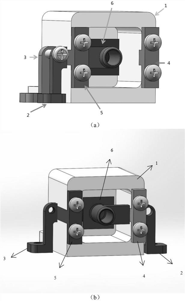
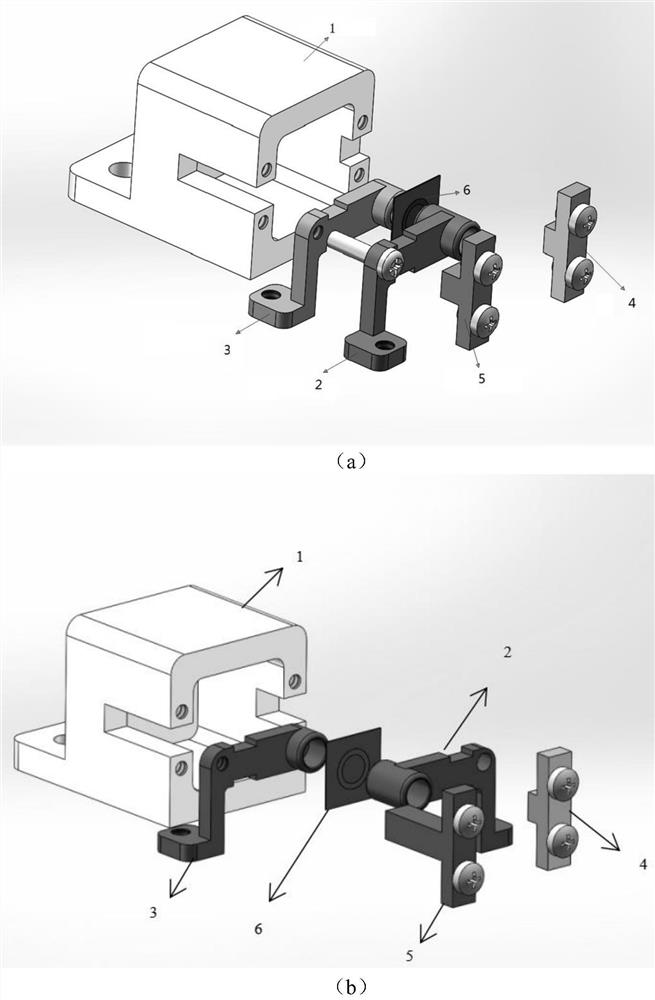
[0030] Such as figure 1 As shown, the present invention consists of an insulating packaging box 1, a positive electrode 2, a negative electrode 3, a first fixing plate 4, a second fixing plate 5, and a SiC wide bandgap photoconductive semiconductor wafer 6 covered with a zinc oxide transparent electrode. Among them, the insulating packaging box 1 is a hollow cube with a deep groove on one side of the cube, and the positive electrode 2 and the negative electrode 3 are stuck in the upper and lower surfaces of the left side of the "factory" through the grooves of the Chinese character "-". In the deep groove, it is pressed and fixed by the second fixed plate 5 with a protrusion in the middle; the positive electrode 2 and the negative electrode 3 are both in the shape of "factory", and a hollow cylinder is arranged at the right end of the "...


PUM


Abstract

The invention specifically relates to a megawatt-level photoconductive semiconductor device and an electrode connection and insulation packaging method for photon microwaves. It is composed of an insulating packaging box, a positive electrode, a negative electrode, a second fixed plate, and a wide bandgap photoconductive semiconductor wafer. The invention takes the photoconductive semiconductor insulating packaging box as the main structure, and solves the problems of ohmic contact and high-voltage resistance insulation between micron-level photoconductive semiconductor devices and external electrodes through electrode coating and insulating glue potting. By optimizing the electrode structure and improving the coating and potting methods, the problem of ohmic contact between the photoconductive semiconductor device and the external circuit is solved, the ohmic contact resistance of the photoconductive semiconductor device is greatly reduced, and the stability of the ohmic contact is also ensured. The invention can effectively improve the withstand voltage and insulation characteristics of the photoconductive semiconductor device and the overall compactness of the system under the pulse width of tens of ns and the repetition frequency of tens of kV and high voltage, and realize the photon microwave output of the megawatt level.

Description

technical field [0001] The invention relates to the fields of optical technology, pulse power technology, high-power microwave technology, etc., and specifically relates to a connection and insulation packaging method of a megawatt-level photoconductive semiconductor device and electrodes for photon microwaves. Background technique [0002] Photoconductive semiconductor devices are one of the key components in the field of pulse power technology for generating high-power ultrashort picosecond pulses. Photoconductive devices not only have the advantages of compact structure of solid-state devices, but also have their own unique advantages, such as extremely fast turn-on time (on the order of picoseconds), extremely small time jitter (on the order of picoseconds), and excellent synchronization Accuracy (picosecond level), low conduction inductance (Yanahen), photoelectric isolation, etc. Especially in terms of power capacity (hundreds of megawatts) and repetition rate (kilohe...

Claims


Application Information

Patent Timeline
Patent Type & Authority Patents(China)
IPC IPC(8): H01L23/043H01L23/10H01L23/18H01L21/52H01L21/54
CPCH01L21/52H01L21/54H01L23/043H01L23/10H01L23/18
Inventor 荀涛楚旭赵昱鑫伍麒霖王日品王朗宁杨汉武贺军涛张军
Owner NAT UNIV OF DEFENSE TECH
Why Eureka
Try Eureka