Slow wave structure based on planar surface plasmon polaritons

A technology of plasmonic polariton and slow wave structure, applied in the field of slow wave structure, can solve the problems of high circuit loss, large conversion structure, difficult processing, etc., achieve high electronic coupling impedance, suitable for mass production, and reduce processing difficulty Effect

Pending Publication Date: 2020-09-01
NANJING UNIV OF INFORMATION SCI & TECH
View PDF5 Cites 4 Cited by
  • Summary
  • Abstract
  • Description
  • Claims
  • Application Information

AI Technical Summary

Problems solved by technology

If the dielectric material is thicker and the dielectric constant of the medium is larger, the electromagnetic field energy will be more concentrated in the dielectric material, and the coupling impedance with electrons will be smaller, resulting in a smaller output power
Second, the input impedance of the microstrip line generally processed by semiconductor technology is relatively high, and the input and input feed structure requires a large conversion structure, which will cause large losses
[0005] The existing millimeter-wave traveling wave tube / return wave tube has the problems of low output power, low efficiency, difficult processing, and high circuit loss

Method used


Image

  • Slow wave structure based on planar surface plasmon polaritons
  • Slow wave structure based on planar surface plasmon polaritons
  • Slow wave structure based on planar surface plasmon polaritons

Examples


Embodiment Construction

[0025] Below in conjunction with accompanying drawing, technical scheme of the present invention is described in further detail:

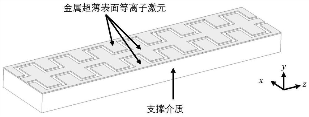
[0026] The invention proposes a novel slow wave structure based on surface plasmon polaritons. As a special transmission line structure, it can support TM surface wave propagation. Since the electronic coupling impedance of the slow wave structure is equal to |E z | - 2 / 2βP, where E z is the radial electric field, β is the propagation constant, and P is the power. The slow wave structure proposed by the present invention has a high radial electric field when the propagation constant and power are constant, so it has a high electronic coupling impedance, and can obtain a relatively large output power in the traveling wave tube / return wave tube. In addition, because the dielectric material used in this slow-wave structure can directly use materials such as silicon germanium commonly used in microelectronics technology, and there is only one lay...


PUM

PropertyMeasurementUnit
electrical conductivityaaaaaaaaaa
relative permittivityaaaaaaaaaa

Abstract

The invention discloses a slow wave structure based on plane surface plasmon polaritons, and relates to the technical field of microwave electric vacuum. The slow wave structure comprises a supportingbase and metal structures, and the metal structures are periodically arranged on the upper surface of the supporting base and comprise a first metal, a second metal and an intermediate metal. The first metal, the second metal and the middle metal are all of surface plasmon polariton structures, the middle metal is arranged between the first metal and the second metal, a certain distance is reserved between the first metal and the middle metal and between the second metal and the middle metal, and the first metal and the second metal are symmetrically distributed relative to the middle metaland are staggered with the middle metal. The slow-wave structure provided by the invention has a very high radial electric field under the condition of a certain propagation constant and power, so that the slow-wave structure has higher electronic coupling impedance, and can obtain the higher output power in a traveling wave tube/backward wave tube.

Description

technical field [0001] The invention relates to the field of microwave electric vacuum technology, in particular to a slow wave structure based on planar surface plasmons. Background technique [0002] Vacuum electronic device is a high-power microwave wave source, which is widely used in radar, guidance, electronic countermeasures, satellite communication and other fields. It is the core of many communication and medical equipment, and its performance directly determines the overall level of equipment. With the rapid development of communication, detection, military defense, and health care, there is an urgent need for high-power, high-reliability, and low-cost millimeter-wave sources. The working principle of vacuum electronic devices is to use the interaction between electrons and electromagnetic fields to generate radiation, and convert the energy of electrons into the energy of electromagnetic waves. Different from microwave solid-state devices widely used at present, ...

Claims


Application Information

Patent Timeline
Patent Type & Authority Applications(China)
IPC IPC(8): H01J23/24H01J25/34
CPCH01J23/24H01J25/34
Inventor 赵晨胡振欣毛伟
Owner NANJING UNIV OF INFORMATION SCI & TECH
Why Eureka
Try Eureka