Inverted light-emitting diode chip and preparation method thereof

A light-emitting diode and chip technology, applied in electrical components, circuits, semiconductor devices, etc., can solve the problems of poor thermal conductivity of sapphire, reduced product reliability, and small total reflection angle of outgoing light, so as to improve the current expansion effect and increase the Recombination area, the effect of improving internal quantum efficiency

Pending Publication Date: 2020-09-11
XIAMEN SILAN ADVANCED COMPOUND SEMICON CO LTD
View PDF0 Cites 5 Cited by
  • Summary
  • Abstract
  • Description
  • Claims
  • Application Information

AI Technical Summary

Problems solved by technology

There are the following disadvantages in the application of front-mounted GaN light-emitting diodes: ①GaN surface emits light, GaN has a high refractive index, and the total reflection angle of the emitted light is small, resulting in a decrease in the ex...

Method used


Image

  • Inverted light-emitting diode chip and preparation method thereof
  • Inverted light-emitting diode chip and preparation method thereof
  • Inverted light-emitting diode chip and preparation method thereof

Examples


no. 2 example

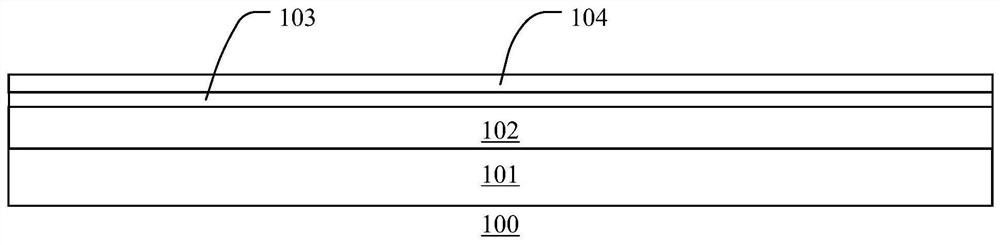
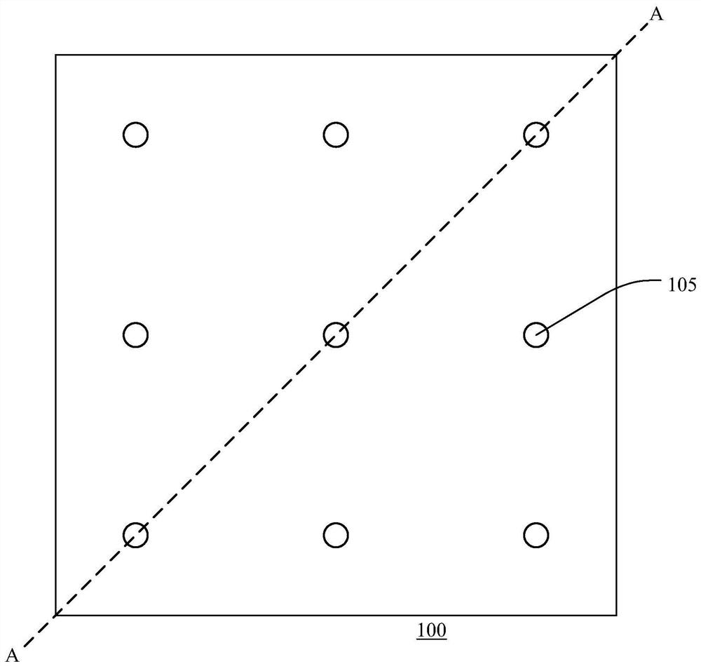
[0098] Such as Figure 9 to Figure 14 As shown, among them, Figure 9 and Figure 12 The dotted line part does not exist, it is only for clearly expressing the structural relationship between the adjacent upper and lower floors. In the second embodiment of the present invention, the flip-chip light-emitting diode chip needs to stack N-type doped gallium nitride layer 102', active layer 103', P-type doped gallium nitride layer 102', P-type doped GaN layer 104' to form a basic semiconductor structure of a flip-chip LED. Further, a current blocking layer 105' is formed on the P-type doped gallium nitride layer 104'. Further, a transparent conductive layer 106' is conformally deposited on the P-type doped gallium nitride layer 104' and the current blocking layer 105'. Further, a layer of photoresist is coated on the transparent conductive layer 106', and then the photoresist is exposed and developed to form an array of openings on the photoresist. Further, part of the transpa...


PUM

PropertyMeasurementUnit
Thicknessaaaaaaaaaa
Thicknessaaaaaaaaaa

Abstract

The invention discloses an inverted light-emitting diode chip and a preparation method thereof. The inverted light-emitting diode chip comprises a substrate; an N-type semiconductor layer, positionedon the substrate; an active layer, positioned on the N-type semiconductor layer; a P-type semiconductor layer, positioned on the active layer; a current spreading layer, positioned on the P-type semiconductor layer; and a first insulating layer, a P electrode, and an N electrode, wherein the first insulating layer is partially located on the current spreading layer and partially penetrates throughthe current spreading layer, the P-type semiconductor layer and the active layer to be in contact with the N-type semiconductor layer. The first insulating layer is provided with a first through holeand a second through hole, the first through hole is located in the current expanding layer, the current expanding layer is connected with the P electrode through the first through hole, the second through hole is located in part of the first insulating layer, and the N-type semiconductor layer is connected with the N electrode through the second through hole. The invention aims to provide the inverted light-emitting diode chip with the array type electrode structure, so that the light-emitting area of the inverted light-emitting diode chip is increased, and the lighting effect of an invertedlight-emitting diode is effectively improved.

Description

technical field [0001] The invention relates to the technical field of light-emitting diodes, in particular to a flip-chip light-emitting diode chip and a preparation method thereof. Background technique [0002] As a solid-state light emitter, gallium nitride-based light-emitting diodes have the advantages of high light efficiency, long life, and low energy consumption. Therefore, gallium nitride-based light-emitting diodes are widely used in full-color display, visible light lighting and other fields. Gallium nitride-based light-emitting diodes usually use sapphire as the substrate, but sapphire is an insulating material. In order to achieve electrical interconnection, the N electrode and the P electrode are located on the gallium nitride surface of the chip, and light is extracted from the gallium nitride surface. This structure It is called a positive gallium nitride-based light-emitting diode. There are the following disadvantages in the application of front-mounted Ga...

Claims


Application Information

Patent Timeline
IPC IPC(8): H01L33/46H01L33/20H01L33/14H01L33/36H01L33/00
CPCH01L33/005H01L33/14H01L33/20H01L33/36H01L33/46
Inventor 赵进超沈丹萍李超马新刚李东昇
Owner XIAMEN SILAN ADVANCED COMPOUND SEMICON CO LTD
Why Eureka
Try Eureka