
Digital signal processor layout distribution positioning method

A digital signal and positioning method technology, applied in the direction of electrical digital data processing, special data processing applications, instruments, etc., can solve the problems of lack of applicability, single function, time-consuming and high cost of reverse analysis methods, and achieve The effect of solving the problem of layout positioning, simple technical thinking, and reducing time and funding costs

Active Publication Date: 2020-09-18
NORTHWEST INST OF NUCLEAR TECH
View PDF9 Cites 2 Cited by
  • Summary
  • Abstract
  • Description
  • Claims
  • Application Information

AI Technical Summary

Problems solved by technology

[0005] Both of the above two reverse analysis methods analyze the layout of commercial electronic chips, but this reverse analysis method is only applicable to storage devices with single chip functions and simple structures. electronic chip
In addition, reverse analysis methods are time and costly
Therefore, reverse analysis is not applicable to large-scale integrated circuits with many functional modules and complex structures.

Method used


Image

  • Digital signal processor layout distribution positioning method
  • Digital signal processor layout distribution positioning method
  • Digital signal processor layout distribution positioning method

Examples


Embodiment Construction

[0032] In order to make the purpose, technical solution and advantages of the present invention clearer, the technical details of the present invention will be described in detail below in conjunction with the accompanying drawings and embodiments. It should be noted that the specific examples are only used to explain the present invention, not to limit the present invention.

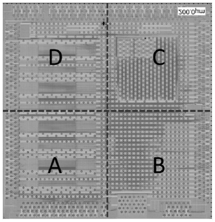
[0033] For ultra-large-scale integrated circuits, especially digital signal processors, the present invention proposes a method for locating the layout distribution of digital signal processors based on the experimental results of heavy ion micro-beams or laser micro-beams combined with chip pin distribution. The method of the present invention is combined with a DSP test system, by carrying out heavy ion micro-beam or laser micro-beam experiments, scanning the layout of the unpackaged DSP chip, and marking the sensitive points where Single Event Effect (SEE) occurs in different modules and effect type....


PUM


Abstract

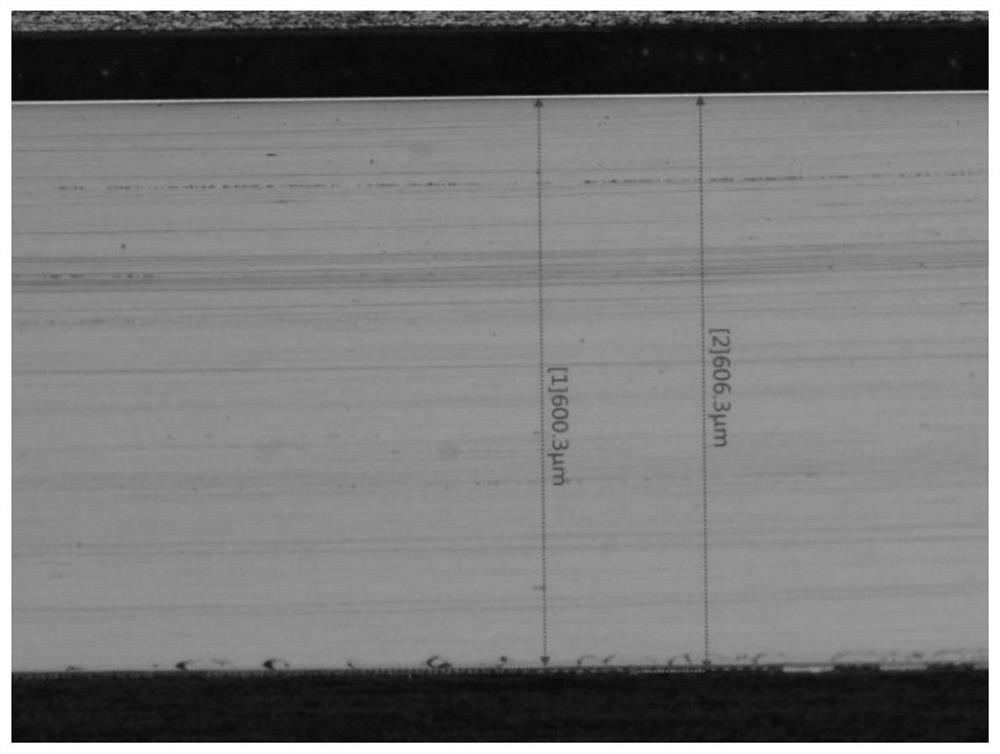
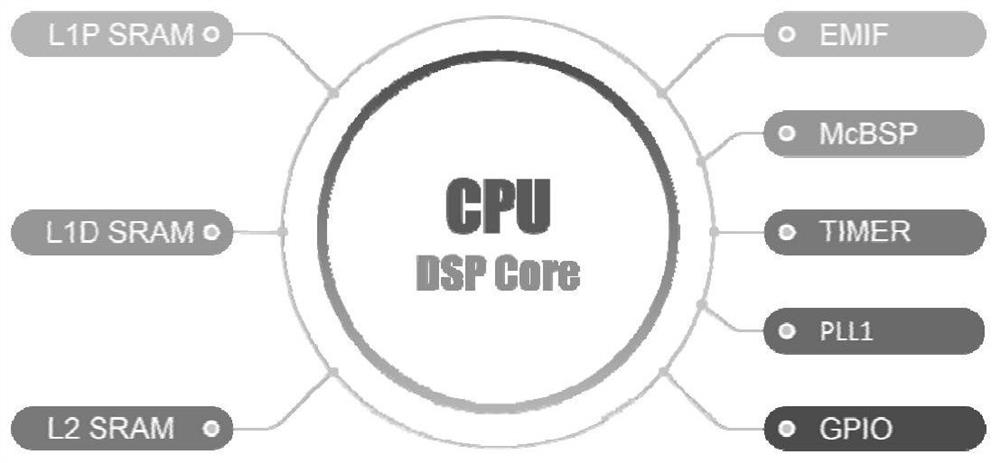
In order to overcome the limitation of an existing reverse analysis method on the applicability of a large-scale integrated circuit, the invention provides a digital signal processor layout distribution positioning method, which comprises the following steps of: 1, acquiring an active region dyeing photograph of a DSP (Digital Signal Processor) chip; 2, if the DSP chip adopts an inverted packagingstructure, thinning and polishing the substrate of the DSP chip; 3, dividing the DSP chip into different modules; 4, positioning a quadrant where each module is located; 5, marking each position coordinate and time information for generating the single event effect; 6, marking all single event effect data points on the original layout photo of the DSP chip according to position coordinates; and 7, confirming the layout positioning of each module according to the acquired single event effect position coordinates, and drawing the position of each module by using a drawing tool in combination with the active region dyeing micrograph.

Description

technical field [0001] The invention belongs to the field of integrated circuit design, and in particular relates to a digital signal processor layout distribution positioning method. Background technique [0002] As a typical VLSI, a digital signal processor (DSP) has the advantages of fast calculation speed, low power consumption, and small size compared with ordinary microprocessors, because of its powerful digital signal Processing plays an important role in digital communication, signal processing, industrial control, image processing and other fields. At the same time, due to the above-mentioned advantages of DSP, it also occupies a very important position in the field of aerospace electronics. [0003] The layout design of integrated circuits is a combination of science and artistry, and it requires long-term practice and accumulation to design excellent products. A good layout design can not only save the volume and weight of the chip, but also optimize the resourc...

Claims


Application Information

Patent Timeline
Patent Type & Authority Applications(China)
IPC IPC(8): G06F30/367
CPCG06F30/392
Inventor 潘霄宇罗尹虹盛江坤张凤祁郭红霞
Owner NORTHWEST INST OF NUCLEAR TECH
Learn More