Laser wafer lift-off device and laser wafer lift-off method

A laser lift-off and wafer technology, applied in laser welding equipment, welding equipment, metal processing equipment, etc., can solve the problems of low work efficiency, reduce the controllability of the processing process, and increase the processing cost, so as to improve quality and efficiency, Eliminate laser processing defects and achieve the effect of secondary processing

Active Publication Date: 2020-09-25
SONGSHAN LAKE MATERIALS LAB +1
View PDF8 Cites 5 Cited by
  • Summary
  • Abstract
  • Description
  • Claims
  • Application Information

AI Technical Summary

Problems solved by technology

At present, wafers are mainly obtained by wire cutting of ingots, but the hard and brittle characteristics of ingot materials lead to defects such as line marks and warping on the processed surface, which need to be removed through subsequent smoothing, grinding, polishing and other processes. low efficiency
In addition, the wear and tear of semiconductor materials and tools is relatively large, which increases the processing cost
[0003] The laser processing method largely avoids a series of problems caused by wire cutting, but this high-energy beam processing method is easy to cause thermal effects on the surface and interior of the material processing, resulting in defects such as microcracks and recast layers. At the same time, laser processing The plasma induced in the process also reduces the controllability of the processing process

Method used


Image

  • Laser wafer lift-off device and laser wafer lift-off method
  • Laser wafer lift-off device and laser wafer lift-off method
  • Laser wafer lift-off device and laser wafer lift-off method

Examples


Embodiment

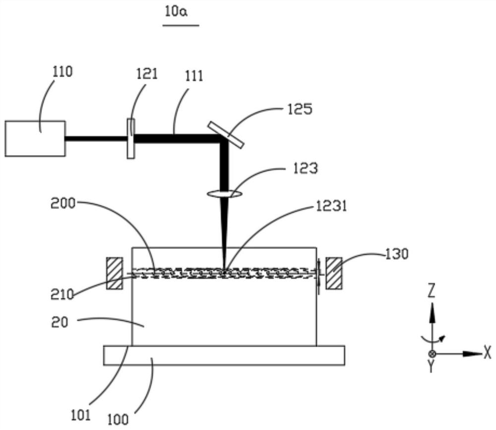
[0043] see figure 1 , a laser lift-off wafer apparatus 10a, which includes: an installation platform 100, a laser emitter 110, a condenser lens assembly, a magnet, and a control system (not shown).

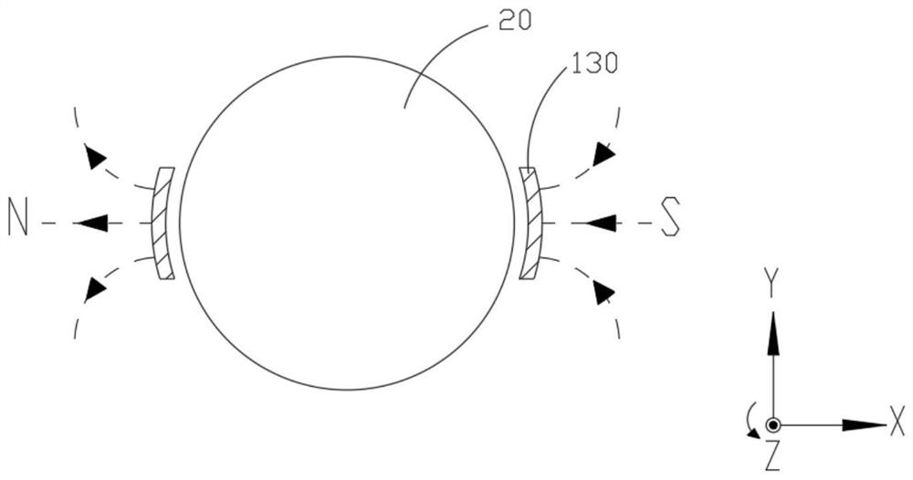
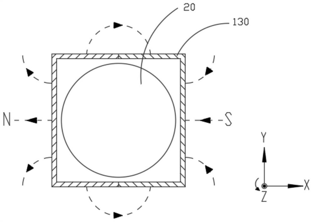
[0044] The installation platform 100 has a bearing surface 101 parallel to the horizontal plane. The bearing surface 101 is used to install and fix the crystal ingot 20 to ensure the stability of the crystal ingot 20 during cutting.

[0045] The laser emitter 110 is used to emit a laser beam, and the laser emitter 110 is specifically, for example, a femtosecond laser, etc., which is not limited herein.

[0046] The focusing lens assembly is used to receive the laser beam 111 emitted by the laser emitter 110 and focus the received laser beam 111 in the crystal ingot 20 to induce the crystal ingot 20 to generate plasma.

[0047] Wherein, the condenser lens assembly includes a beam expander 121 and a focus lens 123, the beam expander 121 receives the laser beam 111 sent by the laser t...


PUM

PropertyMeasurementUnit
thicknessaaaaaaaaaa

Abstract

The invention provides a laser wafer lift-off device and a laser wafer lift-off method, and relates to the field of semiconductor machining. The laser wafer lift-off device comprises an installing platform for installing a crystal ingot, a laser transmitter, a condensing lens assembly, a magnet for providing a magnetic field and a control system. The laser transmitter and the condensing lens assembly are matched to focus laser beams into the crystal ingot so as to induce the crystal ingot to generate a plasma body. The crystal ingot is located in the magnetic field so that the magnetic field can control the motion state of the plasma body. The control system is connected with the magnet. The control system can obtain characteristic parameters of the plasma body in real time and control themagnetic field where the crystal ingot is located in real time according to the characteristic parameters. According to the laser wafer lift-off device and the laser wafer lift-off method, the plasmabody induced by laser is controlled through the magnetic field, the motion process of the plasma body inside the crystal ingot can be changed in real time to perform secondary machining on a modification layer, secondary machining of the machining surface of the wafer is achieved, and the wafer lift-off machining quality and efficiency from the crystal ingot are greatly improved.

Description

technical field [0001] The present application relates to the field of semiconductor processing, in particular, to a laser lift-off wafer device and a laser lift-off wafer method. Background technique [0002] As the basic material of semiconductor devices, wafers are mainly obtained by peeling off crystal ingots, and then processed to obtain substrates or epitaxial wafers to manufacture chips. The thickness of the wafer is usually only on the order of hundreds of microns, and its processing quality is greatly affected by the ingot stripping process. At present, wafers are mainly obtained by wire cutting of ingots, but the hard and brittle characteristics of ingot materials lead to defects such as line marks and warping on the processed surface, which need to be removed through subsequent smoothing, grinding, polishing and other processes. low efficiency. In addition, semiconductor materials and tools wear a lot, which increases the processing cost. [0003] The laser pro...

Claims


Application Information

Patent Timeline
Patent Type & Authority Applications(China)
IPC IPC(8): B23K26/50B23K26/064B23K26/70
CPCB23K26/50B23K26/064B23K26/0643B23K26/702
Inventor 王宏建赵卫朱建海沈旋何自坚申漫漫
Owner SONGSHAN LAKE MATERIALS LAB
Why Eureka
Try Eureka