Supercharge Your Innovation With Domain-Expert AI Agents!

Manufacturing method of micro light-emitting diode display device

A technology of light-emitting diodes and display devices, which is applied in the manufacture of semiconductor/solid-state devices, electrical components, and electrical solid-state devices, etc., and can solve the problems of unable to meet the spacing of electronic components, moving tens of thousands or even hundreds of thousands, and large quantities

Active Publication Date: 2020-09-29
SHENZHEN LONGLI TECH CO LTD
View PDF8 Cites 2 Cited by
  • Summary
  • Abstract
  • Description
  • Claims
  • Application Information

AI Technical Summary

Problems solved by technology

Due to the expansion of the temporary fixed layer in both the horizontal and vertical directions in this method, it is difficult to ensure the accuracy of the horizontal transfer, and it cannot meet the huge transfer with high horizontal precision requirements, and the expansion of the temporary fixed layer is limited, and it cannot meet the large horizontal spacing.
The mass transfer method of Micro-LEDs proposed by Chinese patent CN201711162098 only transfers LEDs with asymmetrical upper and lower edges, and the use of pre-designed molds cannot meet the spacing of electronic components
The problems encountered by these technologies are: 1) The size of the transferred Micro-LED chips is extremely small (3μm-10μm), which requires extremely high-precision operation technology; 2) A transfer needs to move tens of thousands or even hundreds of thousands of Micro-LED chips , the quantity is huge; 3) How to improve the transfer yield to 99.99%, or even higher

Method used


Image

  • Manufacturing method of micro light-emitting diode display device
  • Manufacturing method of micro light-emitting diode display device
  • Manufacturing method of micro light-emitting diode display device

Examples


Embodiment 1

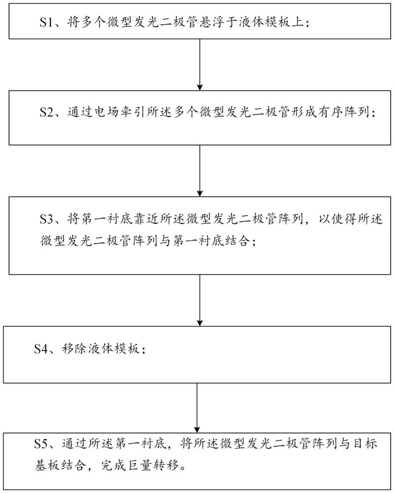
[0035] First, through Figure 1-3 , the method for manufacturing the micro light emitting diode display device according to Embodiment 1 of the present invention will be described. A technical solution adopted in this embodiment is to provide a method for manufacturing a micro light-emitting diode display device, which includes:

[0036] S1. Suspend a plurality of micro light emitting diodes 101 on the liquid template 102, the density of the liquid template 102 ethylene glycol is greater than that of the micro light emitting diodes 101, and the liquid template 102 is expandable. The potentials of the plurality of micro LEDs 101 control their mutual equilibrium distances.

[0037]S2. Pulling the plurality of micro light emitting diodes 101 to form an ordered array by an electric field.

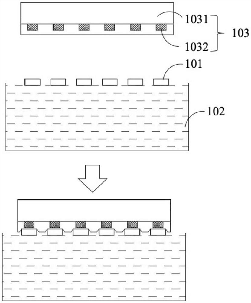
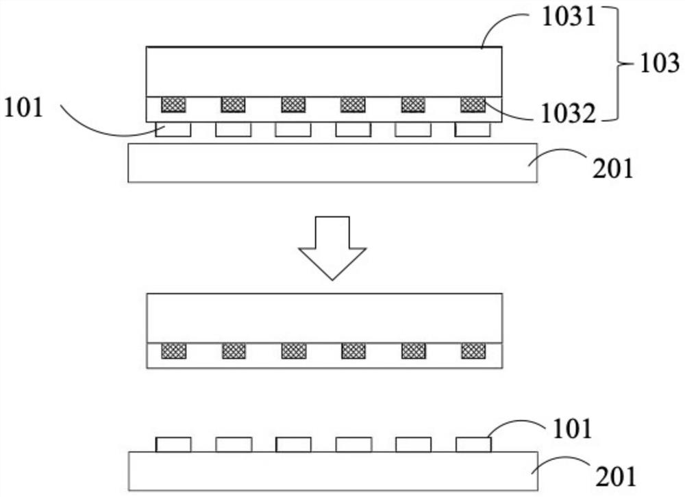
[0038] S3, bringing the first substrate 103 close to the array of micro light emitting diodes 101, so that the array of micro light emitting diodes 101 is combined with the first substrate 10...

Embodiment 2

[0048] Please refer to Figure 4 , is a schematic diagram of step S3 of the manufacturing method of the micro light emitting diode 101 display device according to the second embodiment of the present invention. Only the differences between Embodiment 2 and Embodiment 1 will be described below, and the similarities will not be repeated here.

[0049] The liquid template 102 is dimethyl sulfoxide, and its density is equal to that of the micro LED 101 .

[0050] Before step S1, the micro LEDs 101 are fixed on a first solid template. The manufacturing method of the micro light emitting diode 101 display device further includes removing the first solid template.

[0051] In step S4, the method of removing the liquid template 102 is UV light evaporation.

Embodiment 3

[0053] Please refer to Figure 5 , is a schematic diagram of step S3 of the manufacturing method of the micro light emitting diode 101 display device according to the third embodiment of the present invention. In the following, only the differences between Embodiment 3 and Embodiment 1 will be described, and the similarities will not be repeated here.

[0054] The liquid template 102 is tetrahydrofuran, and its density is smaller than that of the micro LED 101 .


PUM


Abstract

The invention discloses a manufacturing method of a micro light-emitting diode display device. The method comprises the following steps: suspending a plurality of micro light-emitting diodes on a liquid template; pulling the plurality of micro light-emitting diodes to form an ordered array through an electric field; enabling a first substrate to be close to the micro light-emitting diode array, soas to enable the micro light-emitting diode array to be combined with the first substrate; removing the liquid template; and combining the micro light-emitting diode array with a target substrate through the first substrate to complete mass transfer. According to the invention, a huge amount of micro light-emitting diodes can be simply, rapidly and accurately transferred, and the yield is high.

Description

technical field [0001] The invention relates to the manufacture of a display device, in particular to a method for manufacturing a micro light-emitting diode display device. Background technique [0002] Micro-LED (Micro-LED) is "micro" LED (light-emitting diode). Micro-LED array display is a new display technology, and other display technologies, such as liquid crystal display (Liquid Crystal Display, LCD), organic electromechanical laser display (OrganicLight-Emitting Diode, OLED) Plasma Display (PlasmaDisplayPanel, PDP), etc., the core difference is that it uses inorganic LEDs as light-emitting pixels. [0003] The tiny LEDs that have been fabricated need to be transferred to the substrate on which the driving circuit is prepared. Whether it is a TV or a mobile phone screen, the number of pixels is quite huge. Taking a 55-inch 4K TV as an example, the number of chips that need to be transferred is as high as 24 million (calculated based on 4000x 2000x RGB three-color), e...

Claims


Application Information

Patent Timeline
Patent Type & Authority Applications(China)
IPC IPC(8): H01L21/683H01L21/67H01L27/15H01L33/48H01L33/62
CPCH01L21/6835H01L21/67144H01L27/156H01L33/48H01L33/62H01L2221/68368H01L2933/0033H01L2933/0066
Inventor 张小齐刘政李燕彭益庄世强
Owner SHENZHEN LONGLI TECH CO LTD
Features
  • R&D
  • Intellectual Property
  • Life Sciences
  • Materials
  • Tech Scout
  • Unparalleled Data Quality
  • Higher Quality Content
  • 60% Fewer Hallucinations
Learn More