Method for improving photoelectric property of BLFO/ZnO heterojunction by utilizing ferroelectricity and piezoelectric optoelectronics effects
A technology of optoelectronics and optoelectronic properties, applied in nanotechnology for materials and surface science, nanotechnology for information processing, circuits, etc. Improve the effect of significant and fast response speed
- Summary
- Abstract
- Description
- Claims
- Application Information
AI Technical Summary
Problems solved by technology
Method used
Image
Examples
Embodiment 1
[0039] Embodiment 1. A method for improving the optoelectronic performance of BLFO / ZnO heterojunction by using ferroelectricity and piezoelectric photoelectronics effect, by applying pulse bias voltage to BLFO / ZnO heterojunction device, calling BLFO ferroelectricity, BLFO / ZnO heterojunction After the ferroelectricity of BLFO is invoked by the ZnO heterojunction device, compressive strain is applied to the BLFO / ZnO heterojunction device to introduce the piezoelectric photoelectronic effect, so as to achieve the purpose of simultaneously mobilizing the ferroelectric and piezoelectric photoelectronic effects to enhance the current carrying The total driving force of electrons, and test the optoelectronic performance of BLFO / ZnO heterojunction.
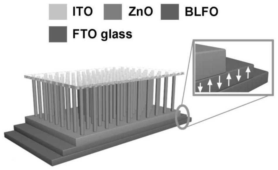
[0040] The BLFO / ZnO heterojunction device is formed by BLFO ferroelectric film and ZnO nanowire array. The upper electrode of the BLFO / ZnO heterojunction device is an ITO electrode prepared by magnetron sputtering. During the sputtering pr...
Embodiment 2
[0048] Embodiment 2, analyzing the BLFO / ZnO heterojunction device.
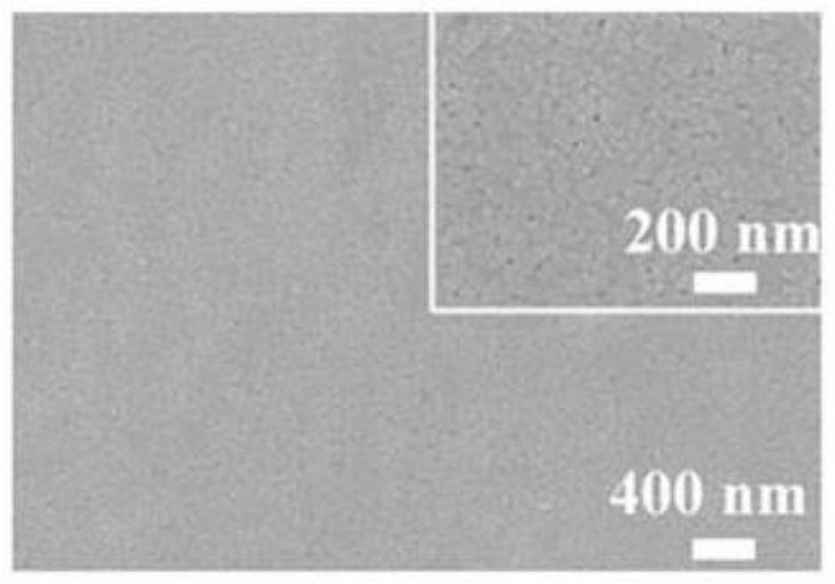
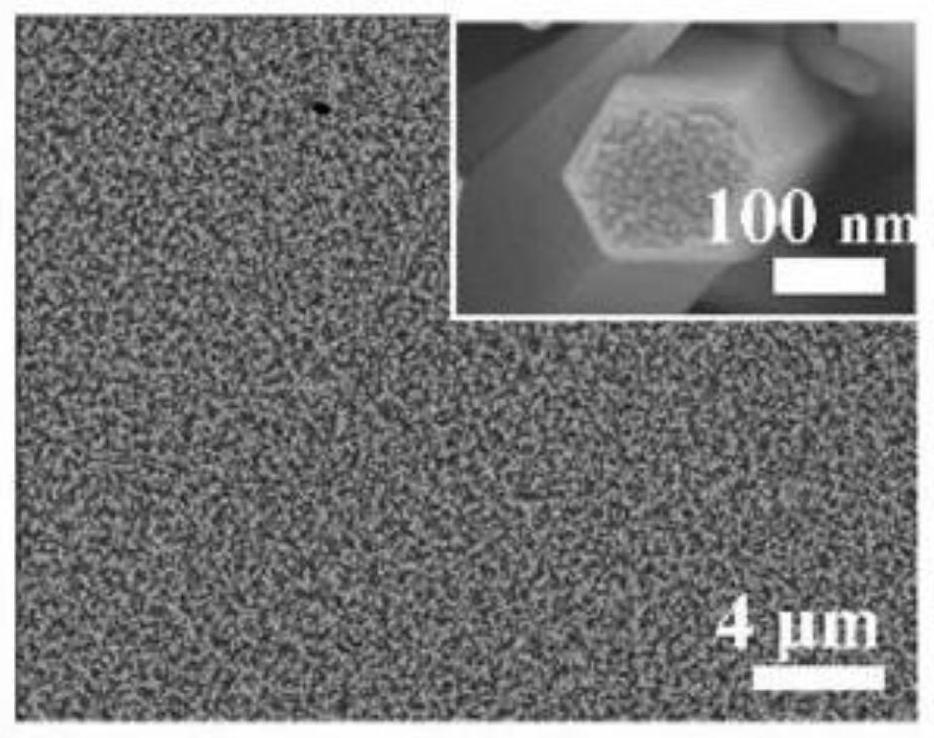
[0049] figure 1 It is a schematic diagram of the three-dimensional structure of a BLFO / ZnO heterojunction device. like figure 2 As shown, the surface of the BLFO film prepared by the sol-gel method in this application is dense, the grain size is uniform, and it has good planarity. Thus, in image 3 In the SEM top view of the ZnO nanowire array in , the ZnO nanowire array is evenly distributed, and it can be seen from the illustration that the top surface of the zinc oxide nanowire has a hexagonal crystal structure, with a uniform diameter of about 200nm, so it has a high c-axis Orientation, with good piezoelectric properties. from Figure 4 It can be clearly seen that the thickness of the FTO conductive layer is about 380nm, the thickness of the BLFO film is about 270nm, and the thickness of the ZnO seed layer is about 1 μm. The ZnO nanowire array has a uniform length of about 6 μm. The interface of F...
Embodiment 3
[0050] Embodiment 3. The J-V (current density-voltage) characteristics of the BLFO / ZnO heterojunction device were tested under a series of laser power densities to verify that it has a photovoltaic effect.
[0051] Image 6 A schematic diagram showing the measurement of photovoltaic characteristics, Figure 7 The schematic diagram of photovoltaic characteristic measurement is shown, and the J-V characteristics of BLFO / ZnO under different light conditions are tested and recorded. like Figure 7 As shown, the photovoltaic characteristics of BLFO / ZnO heterojunction devices gradually increase with the increase of laser power density. Photovoltaic properties of BLFO / ZnO heterojunction devices. When a heterojunction device is biased with a negative (positive) pulse on top of the ITO transparent electrode, it is defined as upward (downward) polarization. Figure 9 It can be clearly seen that there are differences in the photovoltaic characteristics under different polarization st...
PUM
| Property | Measurement | Unit |
|---|---|---|
| size | aaaaa | aaaaa |
| thickness | aaaaa | aaaaa |
| thickness | aaaaa | aaaaa |
Abstract
Description
Claims
Application Information


