Micro light-emitting diode backboard and manufacturing method thereof
A technology for light-emitting diodes and a manufacturing method, which is applied to electrical components, electrical solid-state devices, circuits, etc., can solve the problems of easy peeling cracks, high interface trap density, and complicated process methods, and achieves reduction of sidewall leakage current and light emitting surface. The effect of roughening and improving the luminous efficiency
- Summary
- Abstract
- Description
- Claims
- Application Information
AI Technical Summary
Problems solved by technology
Method used
Image

Examples
no. 1 example
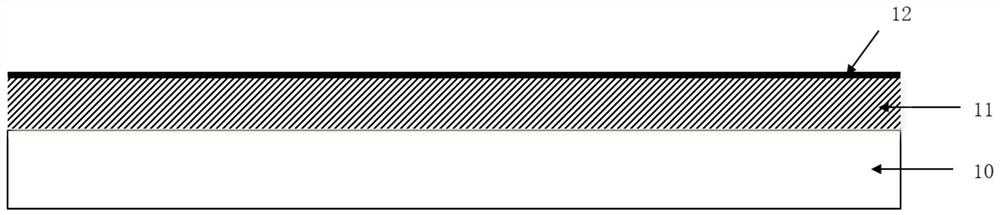
[0049] In the first embodiment, using photoelectrochemistry at room temperature to oxidize the metal gallium layer can be achieved by immersing the transient substrate 20 deposited on the metal gallium layer in an acid solution, or an alkali solution or an aqueous solution, supplemented by an external voltage and ultraviolet light , forming gallium oxide layer 31, its chemical formula is as follows:
[0050] 2GaN+6h + +6OH - → Ga 2 o 3 +3H 2 O+N 2 ↑.
no. 2 example
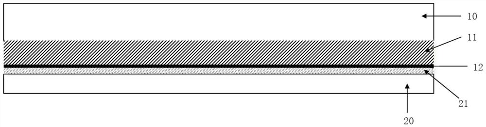
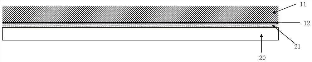
[0051] In the second embodiment, the oxidation is carried out in a high temperature and high oxygen environment. The high temperature can promote the detachment of N atoms, and the reaction of Ga atoms and O atoms produces the gallium oxide layer 31 .
[0052] In the second embodiment, the gallium oxide layer 31 is formed by oxygen plasma treatment.
[0053] After oxidizing the gallium nitride material layer to form the gallium oxide layer 31 by one of the above methods, you can also choose to deposit gallium oxide on the gallium oxide layer 31 formed after the gallium nitride material layer is oxidized to form a thickened gallium oxide layer. layer, so as to achieve the purpose of thickening, of course, this step may or may not be included.
[0054] The present invention also provides a micro LED backplane, such as Figure 7 As shown, it includes a backplane 40, a plurality of bonding metal layers 41 respectively arrayed on the backplane 40, a lower contact electrode 121 bon...
PUM
 Abstract
Description
Claims
Application Information
 - Generate Ideas
- Intellectual Property
- Life Sciences
- Materials
- Tech Scout
- Unparalleled Data Quality
- Higher Quality Content
- 60% Fewer Hallucinations
Browse by: Latest US Patents, China's latest patents, Technical Efficacy Thesaurus, Application Domain, Technology Topic, Popular Technical Reports.
© 2025 PatSnap. All rights reserved.Legal|Privacy policy|Modern Slavery Act Transparency Statement|Sitemap|About US| Contact US: help@patsnap.com