Eureka AIR delivers breakthrough ideas for toughest innovation challenges, trusted by R&D personnel around the world.

Surface plasmon GaN-based LED epitaxial structure and preparation method and application thereof

A surface plasmon and epitaxial structure technology, applied in the direction of electrical components, circuits, semiconductor devices, etc., to achieve efficient coupling, increase the rate of radiation recombination, and maximize the coupling effect

Active Publication Date: 2020-10-13
INST OF SEMICONDUCTORS - CHINESE ACAD OF SCI
View PDF16 Cites 2 Cited by
  • Summary
  • Abstract
  • Description
  • Claims
  • Application Information

AI Technical Summary

Problems solved by technology

How to achieve more effective coupling between the plasmon and the carriers in the quantum well has become a key issue to further improve the performance of the device, but there is no optimized structure for this

Method used


Image

  • Surface plasmon GaN-based LED epitaxial structure and preparation method and application thereof

Examples


preparation example Construction

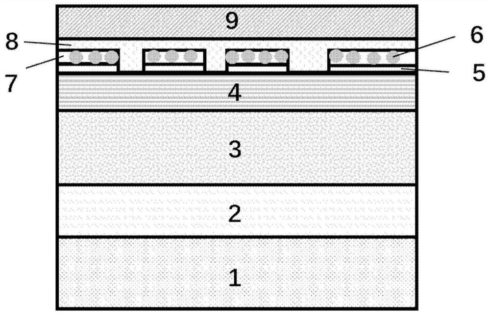
[0057] The invention discloses a method for preparing a surface plasmon GaN-based LED epitaxial structure as described above, including:

[0058] growing a buffer layer on the substrate;

[0059] growing an n-type GaN layer on the buffer layer;

[0060] Growing an InGaN / GaN multi-quantum well active region on the n-type GaN layer;

[0061] Growing a dielectric isolation layer on the InGaN / GaN multi-quantum well active region;

[0062] Depositing a metal layer on the dielectric isolation layer and then thermally annealing it, so that the metal layer is transformed into a metal particle layer;

[0063] Depositing a dielectric cap layer on the metal particle layer, removing part of the dielectric layer, and exposing the upper surface of the InGaN / GaN multiple quantum well active region;

[0064] growing an electron blocking layer on the dielectric cap layer;

[0065] A p-type GaN layer is grown on the electron blocking layer to obtain the epitaxial structure of the surface pl...


PUM

PropertyMeasurementUnit
Thicknessaaaaaaaaaa
Thicknessaaaaaaaaaa
Thicknessaaaaaaaaaa

Abstract

The invention discloses a surface plasmon GaN-based LED epitaxial structure and a preparation method and application thereof. The surface plasmon GaN-based LED epitaxial structure comprises a substrate, a buffer layer, an n type GaN layer, an InGaN / GaN multi-quantum well active region, a dielectric isolation layer, a metal particle layer, a media capping layer, an electron blocking layer, and a ptype GaN layer. The surface plasmon GaN-based LED epitaxial structure provided by the invention comprises no more than three pairs of quantum wells; due to the fact that the coupling efficiency of theplasmon and the quantum well closest to the plasmon, namely the quantum well closest to the pcan, is the highest, maximum coupling of carriers and plasmon coupling can be achieved by reducing the number of the quantum wells, invalid coupling caused by increase of the quantum wells is reduced, and the radiation recombination rate is greatly increased.

Description

technical field [0001] The invention belongs to the field of semiconductor lighting and visible light communication, and in particular relates to a surface plasmon GaN-based LED epitaxy structure and a preparation method and application thereof. Background technique [0002] With the continuous development of visible light communication technology, plasmons have become an important means to improve LED luminescence and modulation characteristics. The mechanism for improving the modulation characteristics of this device is that when the surface plasmon material, such as metal Al, Ag, Au, etc., is close to the active region, the excitons or electron-hole pairs in the active region interact with the surface plasmon A strong coupling effect is generated, so that the excitons or electron-hole pairs transfer energy to the surface plasmons with a very high density of states at an extremely fast rate, and then the surface plasmons convert the energy into photons and radiate them out...

Claims


Application Information

Patent Timeline
IPC IPC(8): H01L33/06H01L33/12H01L33/14H01L33/44H01L33/00
CPCH01L33/06H01L33/12H01L33/44H01L33/145H01L33/0075H01L33/007
Inventor 赵丽霞林杉
Owner INST OF SEMICONDUCTORS - CHINESE ACAD OF SCI
Why Eureka
Eureka Blog
Learn More