WOLED device, manufacturing method thereof and WOLED display device

A technology for a device and a light-emitting layer, which is applied in the field of a WOLED device, a manufacturing method thereof, and a WOLED display device, can solve the problems of aggravated crosstalk, low device efficiency, and further research on WOLED devices.

Pending Publication Date: 2020-10-16
BOE TECH GRP CO LTD
View PDF9 Cites 2 Cited by
  • Summary
  • Abstract
  • Description
  • Claims
  • Application Information

AI Technical Summary

Problems solved by technology

The development and transfer of 2-stack WOLED (2-stacked white light) devices has high brightness and low power consumption, but there are still problems of aggravated crosstalk and high cost; 1-stackWOLD (1-stacked white light) has fewer layers and less quantity The production cycle is short, the production capacity can be increased, and it can meet the needs of some low-brightness products (500nits) customers
The existing 1-stack WOLED mainly has two structu...

Method used


Image

  • WOLED device, manufacturing method thereof and WOLED display device
  • WOLED device, manufacturing method thereof and WOLED display device
  • WOLED device, manufacturing method thereof and WOLED display device

Examples


Embodiment Construction

[0031] Embodiments of the present invention are described in detail below. The embodiments described below are exemplary only for explaining the present invention and should not be construed as limiting the present invention. If no specific technique or condition is indicated in the examples, it shall be carried out according to the technique or condition described in the literature in this field or according to the product specification. The reagents or instruments used were not indicated by the manufacturer, and they were all commercially available conventional products.

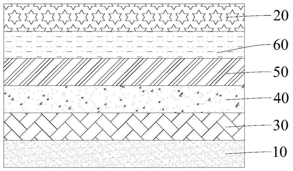
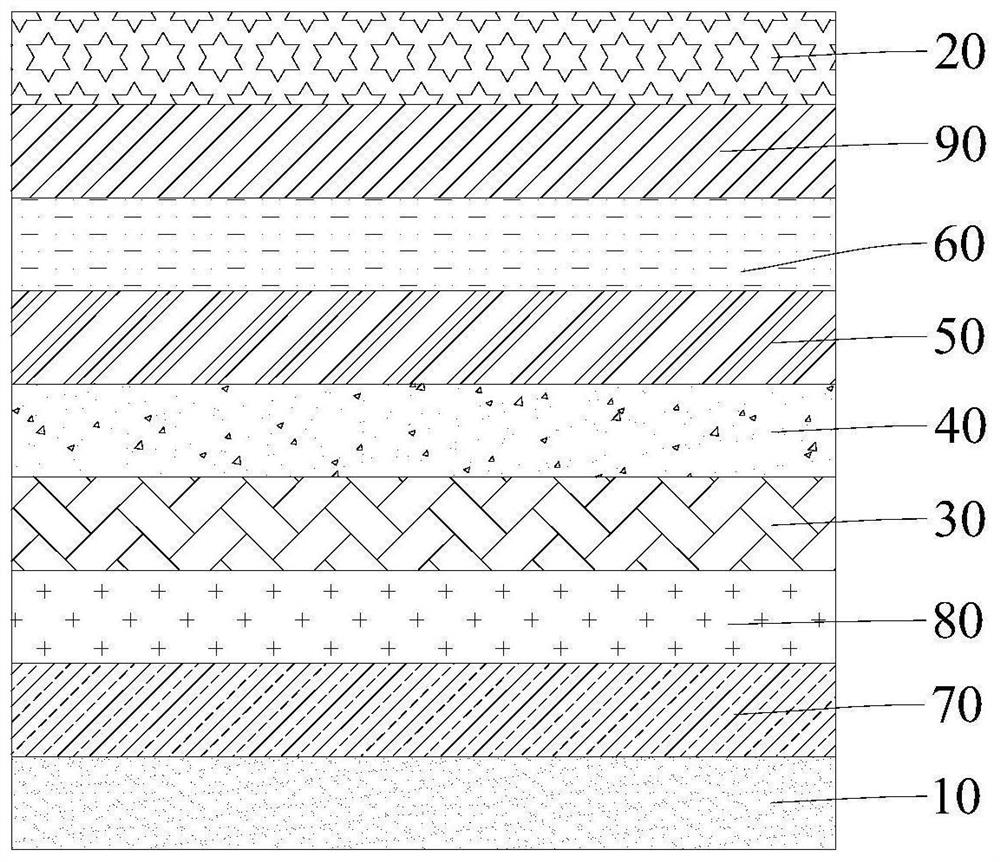
[0032] In one aspect of the invention, the invention provides a WOLED device. According to an embodiment of the present invention, refer to figure 1 , the WOLED device includes: an anode 10; a cathode 20, the cathode 20 is arranged opposite to the anode 10; a red fluorescent light-emitting layer 30, and the red fluorescent light-emitting layer 30 is arranged on the side of the anode 10 close to the catho...


PUM

PropertyMeasurementUnit
Peak wavelengthaaaaaaaaaa
Thicknessaaaaaaaaaa
Electron mobilityaaaaaaaaaa

Abstract

The invention provides a WOLED device, a manufacturing method thereof and a WOLED display device. The WOLED device comprises a cathode and an anode which are arranged oppositely; a red fluorescent light-emitting layer arranged at the side, close to the cathode, of the anode; a green fluorescent light-emitting layer arranged on the surface, close to the cathode, of the red fluorescent light-emitting layer; a spacer layer arranged on the surface, close to the cathode, of the green fluorescent light-emitting layer and comprising a first main body material and a first thermal delay fluorescent material; and blue fluorescent light-emitting layer arranged on the surface, close to the cathode, of the spacer layer. The first main body material and the first thermal delay fluorescent material in the spacer layer of the WOLED device have relatively high triplet state and singlet state, in the TADF material, the energy difference between S1 and T1 energy states is very small, excitons in the T1 state can jump to S1 in an intersystem manner, and then transition from the S1 state to a ground state is carried out to carry out composite luminescence. The TADF plays a role in exciton collection, so that T1 excitons which originally cannot emit light in a transition manner are converted into S1 excitons, and 100% of S1 excitons are formed; the WOLED device is in a full-fluorescence light emitting mode and has a longer service life.

Description

technical field [0001] The invention relates to the field of display technology, in particular, to a WOLED device, a manufacturing method thereof, and a WOLED display device. Background technique [0002] T / E WOLED has attracted extensive attention in the field of organic flat panel display, especially in the field of ultra-high PPI microdisplay, due to its advantages of high resolution, large aperture ratio and flexible substrate selection. Currently, 2-stack WOLED is the mainstream device structure for realizing white light. The development and transfer of 2-stack WOLED (2-stacked white light) devices has high brightness and low power consumption, but there are still problems of aggravated crosstalk and high cost; 1-stackWOLD (1-stacked white light) has fewer layers and less quantity The production cycle is short, and the production capacity can be increased, which can meet the needs of some low-brightness products (500nits) customers. [0003] The 1-stack WOLED has only...

Claims


Application Information

Patent Timeline
IPC IPC(8): H01L51/52H01L51/54H01L51/56H01L27/32
CPCH10K59/40H10K50/131H10K2102/00H10K71/00H10K50/13H10K2101/20H10K50/125H10K50/15H10K50/16H10K50/17
Inventor 黄清雨陈福栋闫华杰刘文祺焦志强
Owner BOE TECH GRP CO LTD
Why Eureka
Try Eureka