Double-groove type SiC MOSFET structure for high-frequency application and manufacturing method

A dual-trench, high-frequency technology, applied in semiconductor/solid-state device manufacturing, electrical components, circuits, etc., can solve problems such as reducing device switching speed, unfavorable high-frequency applications, and increasing switching loss.

Active Publication Date: 2020-10-20
TSINGHUA UNIV
View PDF4 Cites 5 Cited by
  • Summary
  • Abstract
  • Description
  • Claims
  • Application Information

AI Technical Summary

Problems solved by technology

Although this double-trench structure can achieve a better compromise between breakdown voltage and on-resistance, the electric field at the bottom of the trench is still high, and there are still gate oxide reliability issues
At the same time, it also has high gate-to-drain capacitance, which will also reduce the switching speed of the device and increase switching loss, which is not conducive to high-frequency applications

Method used


Image

  • Double-groove type SiC MOSFET structure for high-frequency application and manufacturing method
  • Double-groove type SiC MOSFET structure for high-frequency application and manufacturing method
  • Double-groove type SiC MOSFET structure for high-frequency application and manufacturing method

Examples


Embodiment Construction

[0033]Embodiments of the present invention are described in detail below, examples of which are shown in the drawings, wherein the same or similar reference numerals designate the same or similar elements or elements having the same or similar functions throughout. The embodiments described below by referring to the figures are exemplary and are intended to explain the present invention and should not be construed as limiting the present invention.

[0034] The following describes the structure and preparation method of the double-groove SiC MOSFET for high-frequency applications according to the embodiments of the present invention with reference to the accompanying drawings. First, the double-groove SiC MOSFET for high-frequency applications according to the embodiments of the present invention will be described with reference to the drawings MOSFET structure.

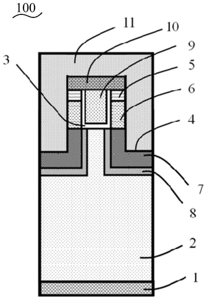
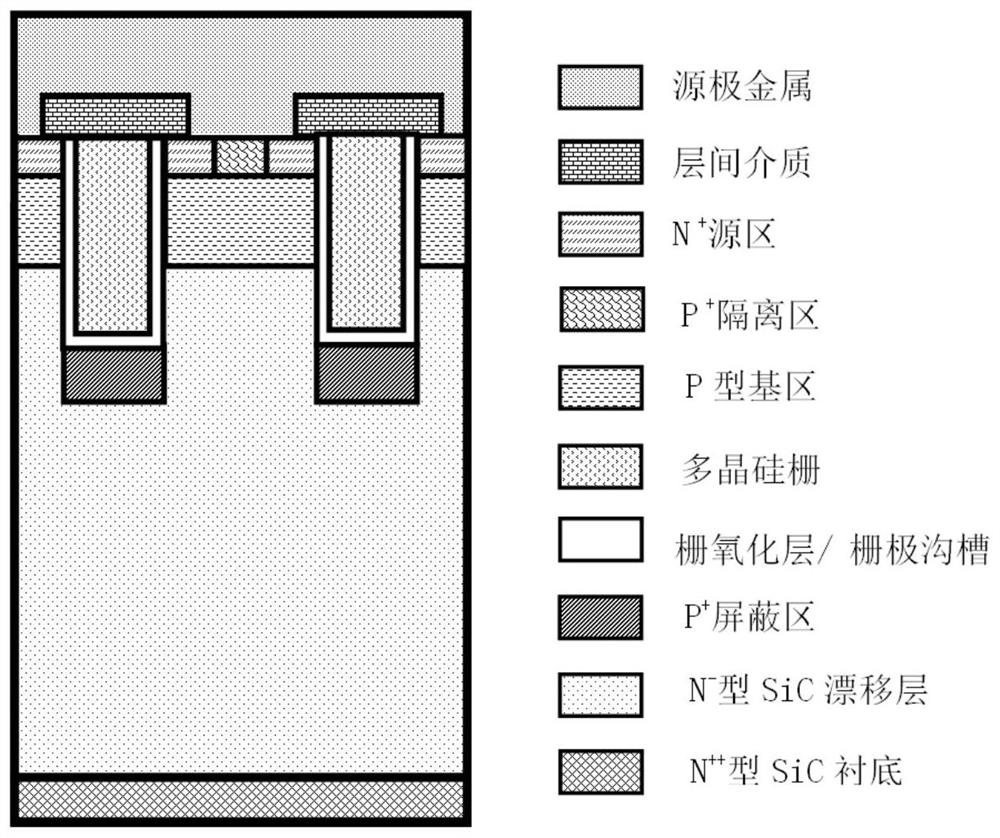
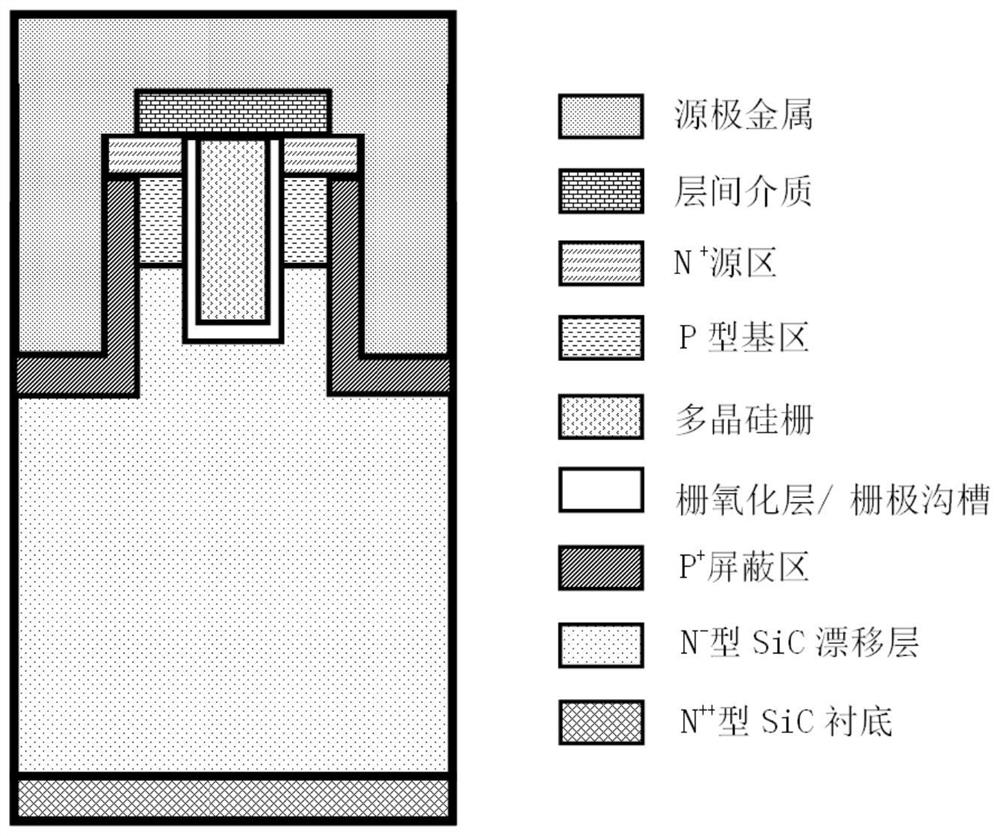
[0035] figure 1 It is a schematic diagram of a double-trench SiC MOSFET structure for high-frequency applications...


PUM

PropertyMeasurementUnit
depthaaaaaaaaaa
thicknessaaaaaaaaaa

Abstract

The invention discloses a double-groove type SiC MOSFET structure for high-frequency application and a manufacturing method. The double-groove type SiC MOSFET structure is constructed on an N-type SiCepitaxial layer on an N++ type SiC substrate, and comprises a gate trench, a source trench, an N + source region, a P-type base region, a P+ shielding region, an N-type current expansion region and an N-type epitaxial layer, wherein the N + source region and the P-type base region are arranged from top to bottom, the P + shielding region is located below the P-type base region and the source trench, the N-type current expansion region is located on the outer side of the P + shielding region, and the N-type epitaxial layer is located in the middle region of the bottom of the gate trench and below the N-type current expansion region. The structure not only has excellent static quality factors of a traditional double-groove type SiC MOSFET, but also can obviously reduce the switching loss and improve the short-circuit endurance capability.

Description

technical field [0001] The invention relates to the technical field of semiconductors, in particular to a double-groove SiC MOSFET structure for high-frequency applications and a manufacturing method thereof. Background technique [0002] SiC is a typical third-generation semiconductor material. Compared with Si, it has a larger band gap, higher critical breakdown field strength and higher thermal conductivity. Therefore, compared with traditional Si-based power semiconductor devices, SiC-based power semiconductor devices can achieve high temperature, high voltage and high frequency operation, significantly improve system energy conversion efficiency, reduce system volume and improve system reliability. [0003] Although Si-based IGBT power devices have been widely used in industrial production and living equipment, they have obvious tail current, which increases switching loss on the one hand and limits the maximum operating frequency on the other hand. Therefore, it may b...

Claims


Application Information

Patent Timeline
Patent Type & Authority Applications(China)
IPC IPC(8): H01L29/06H01L29/423H01L29/78H01L21/28H01L21/336
CPCH01L29/0684H01L29/401H01L29/42356H01L29/4236H01L29/66068H01L29/7827
Inventor 岳瑞峰杨同同王燕
Owner TSINGHUA UNIV
Why Eureka
Try Eureka