Self-adaptive SOI LIGBT device

An adaptive and device technology, applied in semiconductor devices, electrical components, circuits, etc., can solve the problems of increasing device design cost and control difficulty

Active Publication Date: 2020-10-23
UNIV OF ELECTRONIC SCI & TECH OF CHINA
View PDF6 Cites 9 Cited by
  • Summary
  • Abstract
  • Description
  • Claims
  • Application Information

AI Technical Summary

Problems solved by technology

However, this structure needs to introduce an additional gate drive contr

Method used


Image

  • Self-adaptive SOI LIGBT device

Examples


Embodiment 1

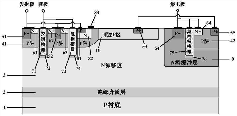
[0019] like figure 1 Shown in this example is an SOI LIGBT device integrated with a Zener diode and a collector NMOS structure.

[0020] This example works as follows:

[0021] When the new device is forward-conducting, there are channels on both sides of the control groove gate and the side of the blocking groove gate close to the emitter, which can increase the channel density of the device, and the blocking groove gate has a physical blocking effect, which can prevent storage in the drift region. The holes in the first P-well region 41 at the emitter end are quickly drawn away by the first P+ body contact region 51 and the second P+ body contact region 52, which is conducive to improving the carrier concentration and current capacity in the drift region to obtain low conduction pressure drop lead. While the collector voltage is relatively low (usually only a few volts) in the conduction state, due to the conductance modulation effect (low resistance effect), the voltage d...


PUM


Abstract

The invention belongs to the technical field of power semiconductors, and particularly relates to a self-adaptive SOI LIGBT device. Compared with a traditional structure, the self-adaptive NMOS structure is introduced into the collector electrode end, and a Zener diode structure is introduced into the emitter electrode end. During forward conduction, the NMOS channel at the collector end is closed, an electron extraction path at the collector end is blocked to eliminate the voltage turn-back effect, and at the moment, the Zener diode is reversely biased but is not broken down, and holes storedin the drift region cannot be extracted, so that the new device can obtain low forward conduction voltage drop. In the turn-off process, along with rise of collector voltage, the collector NMOS channel is adaptively opened to form the electron extraction path, the Zener diode is reversely broken down and conducted to extract an emitter end hole, and the NMOS channel and the Zener diode accelerateturn off of the device to reduce the turn-off loss; and in a short-circuit state, the Zener diode is reversely broken down and conducted, so that the saturation current density can be reduced to improve the short-circuit resistance. Therefore, the device has smaller conduction voltage drop and turn-off loss, and a wider safety working area.

Description

technical field [0001] The invention belongs to the technical field of power semiconductors, and relates to an adaptive SOI LIGBT (Lateral Insulated Gate Bipolar Transistor, lateral insulated gate bipolar transistor) integrated with a Zener diode and a collector NMOS structure. Background technique [0002] Insulated gate bipolar transistor (IGBT) is a gate-controlled bipolar conduction device. Its gate-controlled characteristics make it have the advantages of high input impedance and easy driving. Its bipolar conduction capability makes it easy to achieve low conduction The voltage drop and large current density are very suitable for high-voltage and high-power power electronics technology fields such as smart grids, rail transit, and industrial control. Semiconductor devices based on SOI technology are easy to achieve full dielectric isolation, with lower leakage current and smaller parasitic effects. [0003] The conductance modulation effect occurs in the drift region o...

Claims


Application Information

Patent Timeline
IPC IPC(8): H01L29/739H01L29/06
CPCH01L29/0603H01L29/0611H01L29/7394
Inventor 魏杰郗路凡马臻罗小蓉张波
Owner UNIV OF ELECTRONIC SCI & TECH OF CHINA
Why Eureka
Try Eureka