Chip and forming method thereof

A chip and gate technology, applied in the field of chip and its formation, can solve problems such as difficult to achieve breakdown current, large resistance, affecting chip repair efficiency, etc.

Pending Publication Date: 2020-10-27
CHANGXIN MEMORY TECH INC
View PDF0 Cites 0 Cited by
  • Summary
  • Abstract
  • Description
  • Claims
  • Application Information

AI Technical Summary

Problems solved by technology

[0004] In the prior art, the formation process of the anti-fuse device is relatively complicated, and the resistance during the breakdown process is relatively large, so it is difficult to achieve a large breakdown current, which affects the repair efficiency of the chip

Method used


Image

  • Chip and forming method thereof
  • Chip and forming method thereof
  • Chip and forming method thereof

Examples


Embodiment Construction

[0020] Specific implementations of the antifuse device and its forming method, the memory and its forming method provided by the present invention will be described in detail below in conjunction with the accompanying drawings.

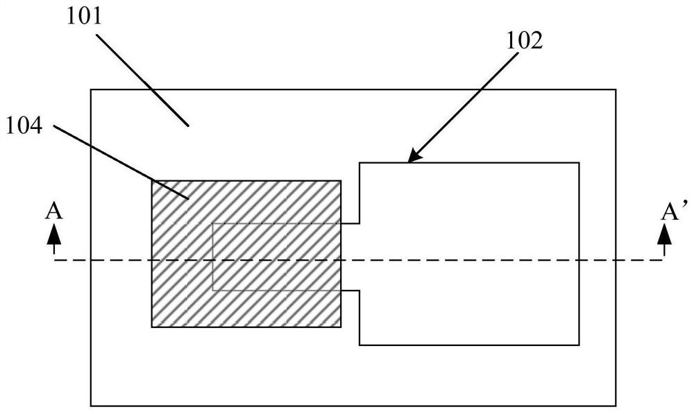
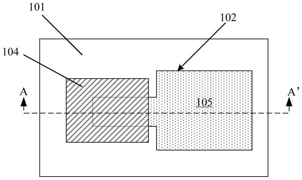
[0021] Please refer to Figure 1 to Figure 4 , is a structural schematic diagram of the formation process of the anti-fuse device according to a specific embodiment of the present invention.

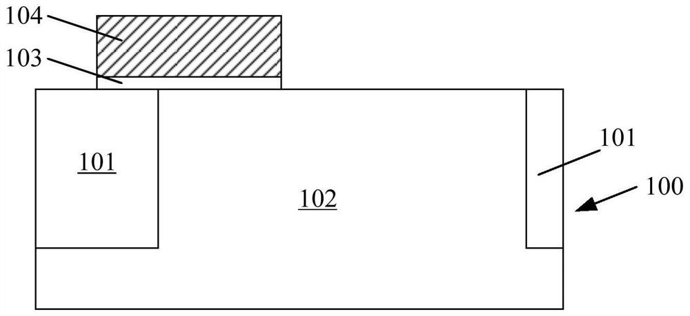
[0022] Please refer to figure 1 and figure 2 ,in figure 2 for along figure 1 Schematic cross-sectional view of the secant line AA'.

[0023] A substrate 100 is provided, and a gate structure is formed on the surface of the substrate 100 . The gate structure includes a gate dielectric layer 103 on the surface of the substrate 100 and a gate 104 on the surface of the gate dielectric layer 103 .

[0024] The substrate 100 may be a semiconductor substrate, such as a single crystal silicon substrate, a single crystal germanium substrate, and the like. The su...


PUM


Abstract

The invention provides a chip and a method of forming the same. The chip includes: a substrate including a storage region and a peripheral region; a storage array formed in the storage region; at least one anti-fuse device formed in the peripheral region and used for repairing a storage defect caused by a failure storage unit in the storage array, wherein the anti-fuse device comprises a gate structure located on the surface of the substrate, and the gate structure comprises a gate dielectric layer located on the surface of the substrate and a gate located on the surface of the gate dielectriclayer; and a doped region arranged in the substrate on one side of the gate structure parallel to the surface direction of the substrate, wherein at least part of the edge of the doped region is aligned with the edge of the gate or is positioned below the gate, and the anti-fuse device is easier to be broken down.

Description

technical field [0001] The invention relates to the field of storage technology, in particular to a chip and a forming method thereof. Background technique [0002] DRAM chips manufactured by semiconductor manufacturing process will inevitably produce defective memory cells, and redundant memory cells are usually formed on the DRAM chip, and the redundant memory cells can be used to permanently replace the defective memory cells to repair the DRAM chip. [0003] When repairing a DRAM chip, one time programming (OTP, one timeprogram) devices such as fuses or antifuses are needed. With the reduction of the feature size of the semiconductor process, the thickness of the gate dielectric layer of the MOS transistor structure is very thin, so that the MOS structure can be used as an anti-fuse device. [0004] In the prior art, the formation process of the anti-fuse device is relatively complicated, and the resistance in the breakdown process is relatively large, so it is difficul...

Claims


Application Information

Patent Timeline
IPC IPC(8): H01L23/525
CPCH01L23/5252
Inventor 刘志拯
Owner CHANGXIN MEMORY TECH INC
Why Eureka
Try Eureka