Shield gate trench power device and manufacturing method thereof

A technology for power devices and shielding gates, applied in the manufacture of semiconductor/solid-state devices, semiconductor devices, electrical components, etc., can solve the problems of increased overlapping area, increased Cgs, etc., to reduce on-resistance, improve thickness uniformity, Effect of Doping Concentration Increase

Active Publication Date: 2020-11-03
SHANGHAI HUAHONG GRACE SEMICON MFG CORP
View PDF10 Cites 8 Cited by
  • Summary
  • Abstract
  • Description
  • Claims
  • Application Information

AI Technical Summary

Problems solved by technology

This bottom tip structure 206 will finally increase the gate-source capacitance Cgs of the device, because the thickness of the shielding dielectric layer in the bottom tip structure 206 will be thinned and the polysilicon gate will be filled to make the intersection between the polysilicon gate and the source polysilicon 204 The stack area increases, these two factors will increase the Cgs

Method used


Image

  • Shield gate trench power device and manufacturing method thereof
  • Shield gate trench power device and manufacturing method thereof
  • Shield gate trench power device and manufacturing method thereof

Examples


Embodiment Construction

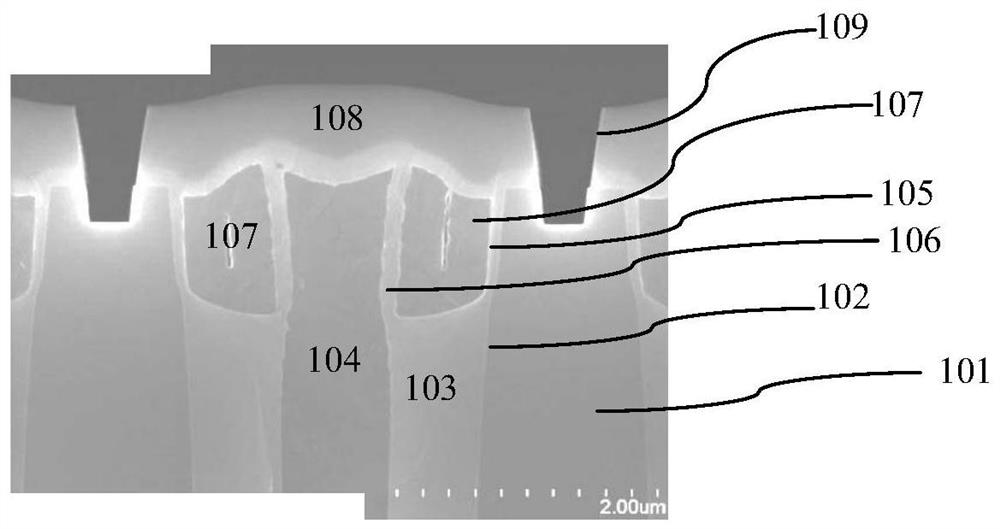
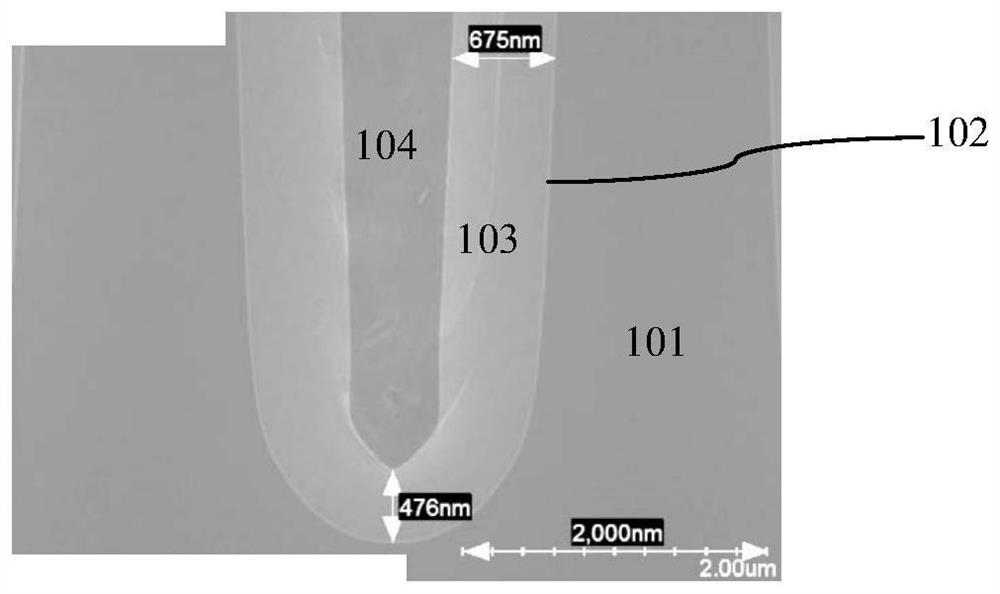
[0074] Such as image 3 Shown is a schematic structural diagram of a shielded gate trench power device according to an embodiment of the present invention; image 3 Only one gate structure is shown in the device unit region 401 in , in fact, the device unit region 401 includes a plurality of device units, and each device unit is provided with a gate structure. The gate structure of the device unit region 401 of the shielded gate trench power device in the embodiment of the present invention includes:

[0075] The epitaxial layer 2 doped with the first conductivity type is formed on the semiconductor substrate 1 , and a gate trench 301 is formed in the epitaxial layer 2 . image 3 In , the semiconductor substrate 1 is also represented by SUB, and the epitaxial layer 2 is also represented by EPI.

[0076] In the embodiment of the present invention, the semiconductor substrate 1 includes a silicon substrate, and the epitaxial layer 2 is a silicon epitaxial layer 2 .

[0077] A...


PUM


Abstract

The invention discloses a shield gate trench power device. A gate structure of a device unit region comprises a shielding dielectric layer formed on the inner side surface of a gate trench; the shielding dielectric layer is formed by superposing a thermal oxidation layer and a CVD dielectric layer; active polycrystalline silicon is filled in a gap region formed by filling the shielding dielectriclayer; top trenches formed by etching part of the shielding dielectric layer close to the side surface of the gate trench are formed in two sides of the source polysilicon, and the top trenches are completely located in the thermal oxide layer; the shielding dielectric layer between the second side surface of the top trench and the source polysilicon is used as an inter-polysilicon dielectric layer; the top trench is filled with a polysilicon gate, and a gate dielectric layer is formed on the first side surface of the top trench. The invention further discloses a manufacturing method of the shield gate trench power device. According to the invention, the thickness uniformity of the side wall and the bottom shielding dielectric layer of the trench can be improved, so the voltage resistanceof the device can be ensured, the on resistance of the device can be reduced, and the gate-source capacitance of the device can be reduced.

Description

technical field [0001] The invention relates to the field of semiconductor integrated circuit manufacturing, in particular to a shielded gate (Shield Gate Trench, SGT) gate trench power device. The invention also relates to a manufacturing method of the shielded gate trench power device. Background technique [0002] Such as Figure 1A Shown is a photograph of the top structure of an existing shielded gate trench (SGT) power device; as Figure 1B shown, is Figure 1A The photo of the bottom of the gate structure of the corresponding shielded gate trench power device; the gate structure of the device cell area of ​​the existing shielded gate trench power device includes: [0003] A gate trench 102 is formed in the epitaxial layer 101 . . [0004] A shielding dielectric layer 103 is formed on the bottom surface and side surfaces of the gate trench 102; the shielding dielectric layer 103 is composed of a thermal oxide layer. [0005] The shielding dielectric layer 103 does ...

Claims


Application Information

Patent Timeline
Patent Type & Authority Applications(China)
IPC IPC(8): H01L29/78H01L29/423H01L21/336
CPCH01L29/7813H01L29/4236H01L29/42372H01L29/42376H01L29/66734H01L29/407Y02B70/10H01L21/28194H01L29/0696
Inventor 杨亚锋石磊
Owner SHANGHAI HUAHONG GRACE SEMICON MFG CORP
Why Eureka
Try Eureka