Adaptive hysteresis control converter for enhancing transient characteristics, control method and equipment

A transient characteristic, hysteretic control technology, applied in control/regulation systems, output power conversion devices, DC power input conversion to DC power output, etc. Compensation capability, improving transient characteristics, achieving the effect of stability

Pending Publication Date: 2020-11-06
深圳市凯冠智能科技有限公司
0 Cites 0 Cited by

AI-Extracted Technical Summary

Problems solved by technology

[0006] The other mainly uses an adaptive ramp generating circuit to generate a ramp signal representing the inductor current, and adopts a hysteresis mode of the upper and lower threshol...

Method used

[0051] In an embodiment of the present application, the compensation unit and the processing unit are connected to the input unit and the comparison unit respectively; wherein the compensation unit includes a MOS transistor M3, a MOS transistor M4, and a MOS transistor M5 , an operational amplifier OP3, a capacitor C2, a capacitor C3, an inductance L and a resistor R1; the drain end and the grid end of the MOS transistor M3 are respectively connected to the input unit, and the grid end of the MOS transistor M3 is respectively connected to the grid end of the MOS transistor M4 terminal, the output terminal of the operational amplifier OP3 is connected to the positive input terminal of the operational amplifier OP3, the source terminal of the MOS transistor M3 is respectively connected to the gate terminal and the drain terminal of the MOS transistor M5, the MOS transistor M4 The drain end of the inductor L is connected to the input unit, the source end of the MOS transistor M4 is respectively connected to one end of the capacitor C2 and one end of the capacitor C3, and the source end of the MOS transistor M5 The other end of the capacitor C2, the other end of the inductor L, and one end of the resistor R1 are connected, and the inverting input end of the operational amplifier OP3 is connected to the other end of the capacitor C3 and the other end of the resistor R1 respectively. One end is connected to the comparison unit. Compared with the existing technical scheme of slope compensation for inductor current sampling, the present invention utilizes the characteristics of MOS transistors operating in the linear resistance region to replace traditional RC resistors, so that they can produce different slo...

Abstract

The invention provides an adaptive hysteresis control converter for enhancing transient characteristics, a control method and equipment. The converter is used for converting input electric energy intoelectric energy with controllable voltage or current required by a load, comprises a compensation unit, an input unit, a processing unit and a comparison unit, and is characterized in that the compensation unit and the processing unit are respectively connected with the input unit and the comparison unit. Compared with the existing slope compensation technical scheme of inductive current sampling, the characteristic that the MOS tube works in a linear resistance region is utilized to substitute traditional RC resistors, different slope compensation characteristics are generated under steady-state and transient-state conditions, the stability of the converter in a steady state is realized, the linear resistance value of the MOS is changed by utilizing feedback control in a transient state,the slope compensation capability is improved, the transient characteristic of the hysteresis control converter is improved, and the hysteresis control converter is simple in circuit structure, easyin technical operation and lower in cost.

Application Domain

Dc-dc conversionElectric variable regulation

Technology Topic

PhysicsTransient state +11

Image

  • Adaptive hysteresis control converter for enhancing transient characteristics, control method and equipment
  • Adaptive hysteresis control converter for enhancing transient characteristics, control method and equipment
  • Adaptive hysteresis control converter for enhancing transient characteristics, control method and equipment

Examples

  • Experimental program(1)

Example Embodiment

[0040] In order to make the objectives, features, and advantages of the application more obvious and understandable, the application will be further described in detail below in conjunction with the drawings and specific implementations. Obviously, the described embodiments are part of the embodiments of the present application, rather than all of the embodiments. Based on the embodiments in this application, all other embodiments obtained by a person of ordinary skill in the art without creative work shall fall within the protection scope of this application.
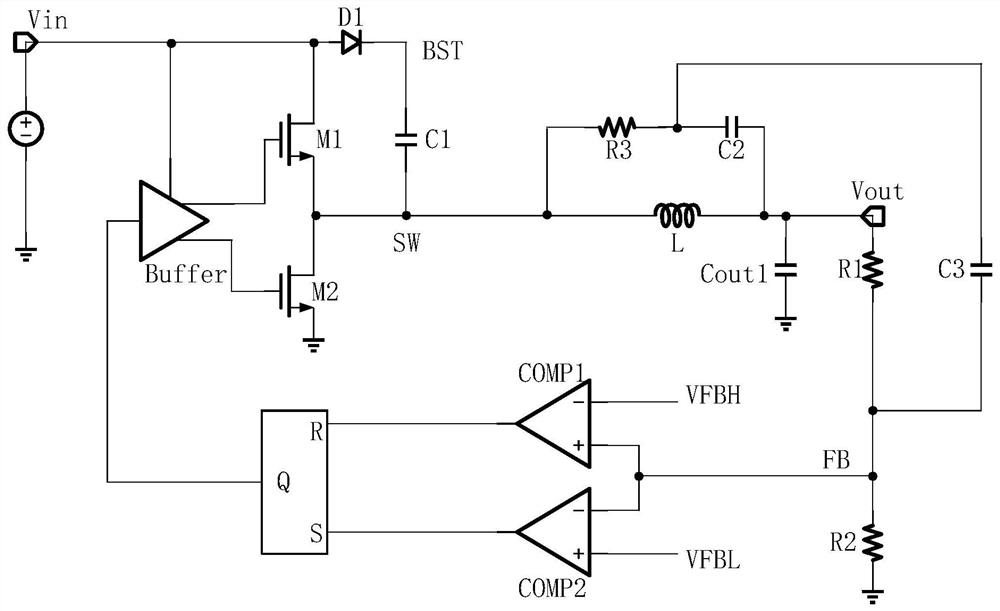
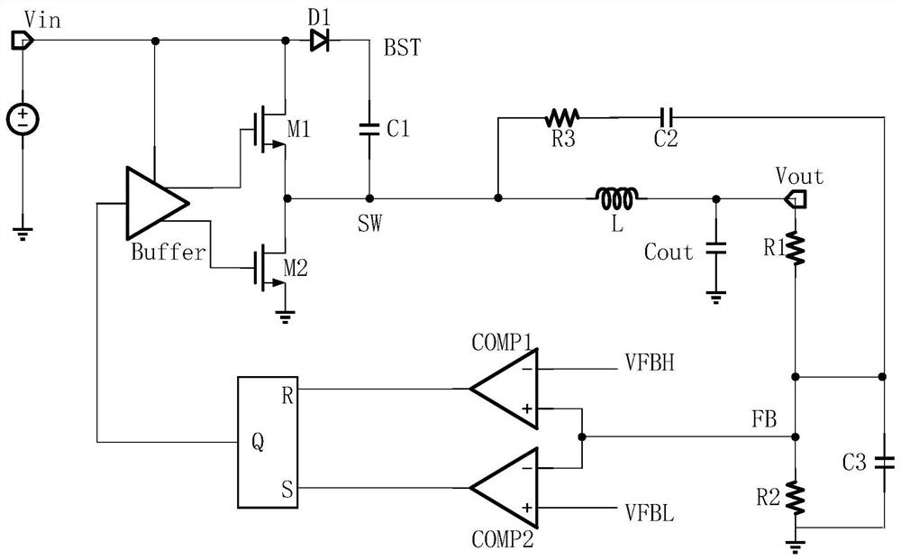
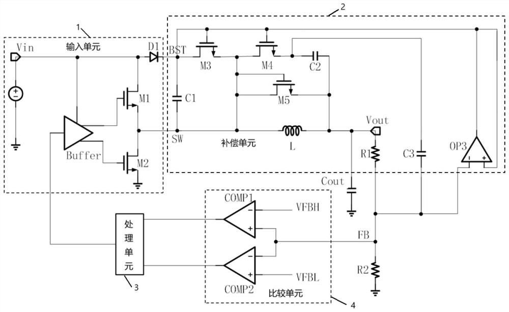
[0041] It should be noted that, in any embodiment of the present invention, the Buck converter is a step-down switching converter; MOS is a metal oxide semiconductor field effect transistor; V FB Is the feedback voltage; FB is the feedback node of the converter; Fs is the switching frequency of the converter; C out Is the output capacitor; Resr is the equivalent internal impedance of the output capacitor; Scomp is the compensation intensity; SW is the switch node of the converter; V GS Is the voltage between the gate and source of the MOS tube; V DS Is the voltage between the drain and source of the MOS tube; V TH Is the threshold voltage of the gate terminal of the MOS tube; OP is an operational amplifier; COMP is a comparator; BST is a bootstrap boost node, which provides power supply voltages for MOS tubes M1, MOS tubes M3, MOS tubes M4, and MOS tubes M5.
[0042] Reference image 3 , Shows an adaptive hysteresis control converter with enhanced transient characteristics provided by an embodiment of the present application. The converter is used to convert input electrical energy into voltage or current controllable electrical energy required by the load, and includes a compensation unit , An input unit, a processing unit and a comparison unit, the compensation unit and the processing unit are respectively connected to the input unit and the comparison unit;
[0043] Wherein, the compensation unit includes MOS tube M3, MOS tube M4, MOS tube M5, operational amplifier OP3, capacitor C2, capacitor C3, inductor L and resistor R1;
[0044] The drain terminal and the gate terminal of the MOS tube M3 are respectively connected to the input unit,
[0045] The gate terminal of the MOS tube M3 is connected to the gate terminal of the MOS tube M4, the output terminal of the operational amplifier OP3, and the forward input terminal of the operational amplifier OP3, respectively,
[0046] The source terminal of the MOS tube M3 is connected to the gate terminal and the drain terminal of the MOS tube M5, the drain terminal of the MOS tube M4, one end of the inductor L, and the input unit, respectively,
[0047] The source end of the MOS transistor M4 is respectively connected to one end of the capacitor C2 and one end of the capacitor C3,
[0048] The source end of the MOS transistor M5 is connected to the other end of the capacitor C2, the other end of the inductor L, and one end of the resistor R1,
[0049] The reverse input end of the operational amplifier OP3 is respectively connected to the other end of the capacitor C3, the other end of the resistor R1 and the comparison unit.
[0050] This application has the following advantages:
[0051] In the embodiment of the present application, the compensation unit and the processing unit are respectively connected to the input unit and the comparison unit; wherein, the compensation unit includes a MOS tube M3, a MOS tube M4, a MOS tube M5, and an operational amplifier OP3, capacitor C2, capacitor C3, inductor L and resistor R1; the drain terminal and gate terminal of the MOS tube M3 are respectively connected to the input unit, and the gate terminal of the MOS tube M3 is connected to the gate terminal and the gate terminal of the MOS tube M4 respectively. The output terminal of the operational amplifier OP3 is connected to the positive input terminal of the operational amplifier OP3, and the source terminal of the MOS tube M3 is respectively connected to the gate terminal and the drain terminal of the MOS tube M5, and the drain terminal of the MOS tube M4. One end of the inductor L is connected to the input unit, the source end of the MOS transistor M4 is connected to one end of the capacitor C2 and one end of the capacitor C3, and the source end of the MOS transistor M5 is connected to the The other end of the capacitor C2, the other end of the inductor L, and one end of the resistor R1 are connected, and the inverting input end of the operational amplifier OP3 is connected to the other end of the capacitor C3, the other end of the resistor R1, and the The comparison unit is connected. Compared with the existing slope compensation technical solution for inductor current sampling, the present invention uses the characteristics of the MOS tube working in the linear resistance region to replace the traditional RC resistance, so that it produces different slope compensation characteristics under steady state and transient conditions. , It not only realizes the stability of the converter in the steady state, but also uses feedback control to change the linear resistance of the MOS in the transient state, improves the slope compensation ability, improves the transient characteristics of the hysteresis control converter, and the circuit structure of the present invention Simple, easy technical operation and lower cost.
[0052] In the following, the method for estimating the logistics path in this exemplary embodiment will be further explained.
[0053] Specifically, the adaptive hysteresis control converter is essentially a ripple feedback control topology. Refer to image 3 Shown.
[0054] From the point of view of electrical characteristics, the feedback ripple can be expressed as:
[0055]
[0056] Because VFBH-VFBL is an approximate constant value, the peak-to-peak value of △VFB is approximately a constant value. Therefore, when the output capacitor only uses ceramic capacitors, its Rser is small, resulting in a small switching frequency Fs, so the transient response will be poor at lower frequencies. In order to improve this problem, the traditional hysteresis control converter will introduce the slope compensation circuit of inductor current sampling to increase the voltage ripple slope of FB, and then increase the switching frequency to achieve better transient response. figure 1 , 2 As shown, by sampling the voltage difference between the two ends of the inductor L or between SW and FB, it is essentially a pseudo-current detection method that represents the current by voltage. R3 and C2 are connected in series to realize constant current charging and discharging of the capacitor, thereby generating a ramp voltage signal △Vripple, superimpose this signal with the output ripple △Vout*[R2/(R1+R2)] obtained by dividing the voltage of R1 and R2 to increase the ripple slope of △VFB, thereby increasing Fs and achieving better transient Response, the superposition process is like Figure 4 Shown.
[0057] According to the capacitor charging and discharging characteristics, the slope compensation intensity Scomp∝1/RC, but the increase of the compensation intensity will directly affect the loop stability, that is, it is difficult to ensure the stability of the converter in the case of overcompensation, so the traditional RC slope compensation There are great limitations to the improvement of transient response. Compared with the traditional slope compensation method adopted by the inductor current, the invention maximizes the transient characteristics under the condition of ensuring the stable operation of the circuit.
[0058] Further, the input unit includes a diode D1, a MOS tube M1, a MOS tube M2, a capacitor C1, and a buffer;
[0059] The buffer Buffer is respectively connected to the gate terminal and the drain terminal of the MOS tube M1, the gate terminal of the MOS tube M2, the processing unit, the input terminal of the diode D1, and the anode of the input power source;
[0060] The drain terminal of the MOS tube M1 is connected to the input terminal of the diode D1; the source terminal of the MOS tube M1 is connected to the drain terminal of the MOS tube M2, the other end of the capacitor C1, and the inductor L One end connected
[0061] The output terminal of the diode D1 is respectively connected to the drain terminal and the gate terminal of the MOS tube M3 and one end of the capacitor C1;
[0062] The source terminal of the MOS tube M2 is grounded.
[0063] Further, the comparison unit includes a comparator COMP1 and a comparator COMP2;
[0064] The output end of the comparator COMP1 is connected to the processing unit; the forward input end of the comparator COMP1 is connected to the other end of the resistor R1; the reverse input end of the comparator COMP1 is connected to the comparison voltage VFBH Input terminal connection;
[0065] The output terminal of the comparator COMP2 is connected to the processing unit; the negative input terminal of the comparator COMP1 is connected to the other terminal of the resistor R1; the forward input terminal of the comparator COMP2 is connected to the comparison voltage VFBL Input terminal connection.
[0066] Further, the MOS tube M3, the MOS tube M4, and the MOS tube M5 are connected in a split series connection to form two clamped tubes, and the MOS tube M5 is a clamped MOS tube.
[0067] Further, the linear resistance of the MOS tube M4 is at V DS4 GS3 -V TH3 The linear resistance area; where V GS3 Is the voltage between the gate and source of the MOS tube M3; V DS4 Is the voltage between drain and source of MOS tube M4; V TH3 It is the threshold voltage of the gate terminal of the MOS tube M3.
[0068] Reference image 3 In the present invention, the resistor R3 in the traditional RC compensation is replaced by a MOS tube M4, so that M4 and C2 form a new RC compensation circuit. M3, M4, and M5 form a clamp split series structure, and the principle of the structure is as follows:
[0069] Under the condition that the working voltage of the structure is guaranteed to work, the connection mode of M3 determines that the saturation condition is unconditionally satisfied. According to the mathematical model of the MOS tube, M3 and M4 must satisfy the following relationship:
[0070] (V GS4 -V TH4 )-V DS4 =(V GS3 +V DS4 -V TH4 )-V DS4 =V DS3 -V TH4
[0071] Due to the offset effect of M3, VTH3≥VTH4, and because M3 is saturated and turned on, VGS3-VTH3>0, so
[0072] VTH3+VGS3-VTH3-VTH4≥VGS3-VTH3>0
[0073] Obviously, it is necessary to satisfy that M4 enters the linear resistance region to reduce the current to meet the condition of continuous current, so M4 must be in the linear resistance region of VDS4
[0074] M5 is a clamped MOS tube, connected in parallel with M4. M5 uses a diode connection to ensure sufficient operating voltage, M5 will not enter the cut-off state and must be in a saturated state, compared to M4, I5 working in the linear region > > I4 realizes the shunting function, which ensures that the M4 tube is always in the linear resistance region, and also ensures that the current flowing through the M4 will not be too large, resulting in over-compensation or excessive value of the C2 capacitor.
[0075] This structure uses BST as a high level to ensure that there is a sufficiently high voltage to make M3 and M5 always work in the saturation region, so that M4 always works in the linear resistance region. Because the voltage across the inductor L is only related to the frequency under small signal conditions, the instantaneous frequency of the transient change is approximately constant, so the voltage across the inductor L is approximately constant, so the small signal impedance of M4 is only controlled by its gate terminal signal, and the gate of M4 The terminal is connected with the output terminal of the operational amplifier OP3, and the sampling voltage is converted from FB through OP3 and quickly fed back to the M4 gate terminal to control its linear resistance.
[0076] Further, the source terminal of the MOS transistor M5 is also grounded through the output capacitor Cout.
[0077] Further, the reverse input terminal of the operational amplifier OP3 is grounded through a resistor R2.
[0078] A control method of an adaptive hysteresis control converter with enhanced transient characteristics,
[0079] When the load is stable, the linear resistance of the MOS tube M4 is kept unchanged.
[0080] Specifically, when the load is stable, the feedback voltage at FB is approximately stable between VFBL and VBFH. At this time, the linear resistance of M4 remains approximately unchanged, and the compensation circuit composed of M4 and C2 can meet the stability requirements of the circuit under steady state. .
[0081] In an embodiment of the present invention, when the load changes from light load to heavy load, the linear resistance of the MOS transistor M4 is reduced.
[0082] Specifically, when the load changes from light load to heavy load, V out An undershoot voltage is formed, and the feedback voltage at FB is pulled down instantaneously by the resistor R1 and resistor R2. At this time, the operational amplifier OP3 quickly samples and quickly pulls up the output of the operational amplifier. According to the working model of MOS working in the linear region,
[0083]
[0084] When the output of the operational amplifier OP3 increases, the V of the MOS tube M4 GS4 Will increase, so its linear resistance R ds4 According to the relationship between the slope compensation intensity and RC, compared with the steady state, the transient slope compensation intensity is greatly increased, and its transient characteristics are further improved.
[0085] In summary, it can be seen that the technical advantages of the adaptive hysteresis control converter with enhanced transient characteristics proposed by the present invention: use the characteristics of the MOS tube to work in the linear resistance region to replace the traditional RC resistor to make it in steady state and transient Different slope compensation characteristics are produced under the condition of low state, that is, it satisfies the stability of the converter in the steady state, and uses feedback control to change the linear resistance of the MOS in the transient state, which improves the slope compensation ability and greatly improves the hysteresis control converter Transient characteristics.
[0086] A device includes an adaptive hysteresis control converter with enhanced transient characteristics as described in any one of the foregoing embodiments.
[0087] Although the preferred embodiments of the embodiments of the present application have been described, those skilled in the art can make additional changes and modifications to these embodiments once they learn the basic creative concept. Therefore, the appended claims are intended to be interpreted as including the preferred embodiments and all changes and modifications falling within the scope of the embodiments of the present application.
[0088] Finally, it should be noted that in this article, relational terms such as first and second are only used to distinguish one entity or operation from another entity or operation, and do not necessarily require or imply these entities Or there is any such actual relationship or sequence between operations. Moreover, the terms "include", "include" or any other variants thereof are intended to cover non-exclusive inclusion, so that a process, method, article, or terminal device that includes a series of elements includes not only those elements, but also those that are not explicitly listed Other elements listed, or also include elements inherent to this process, method, article or terminal device. If there are no more restrictions, the element defined by the sentence "including a..." does not exclude the existence of other same elements in the process, method, article or terminal device that includes the element.
[0089] The above provides a detailed introduction to the adaptive hysteresis control converter, control method, and equipment for enhancing transient characteristics provided by the present application. Specific examples are used in this article to illustrate the principles and implementations of the present application. The description is only used to help understand the methods and core ideas of this application; at the same time, for those of ordinary skill in the art, according to the ideas of this application, there will be changes in the specific implementation and the scope of application. In summary , The content of this specification should not be construed as a limitation to this application.

PUM

no PUM

Description & Claims & Application Information

We can also present the details of the Description, Claims and Application information to help users get a comprehensive understanding of the technical details of the patent, such as background art, summary of invention, brief description of drawings, description of embodiments, and other original content. On the other hand, users can also determine the specific scope of protection of the technology through the list of claims; as well as understand the changes in the life cycle of the technology with the presentation of the patent timeline. Login to view more.

Similar technology patents

Steel bar connecting structure

PendingCN113653036AReduce work intensityachieve stability
Owner:顾东东

Water cooling machine shell heat core box electric heating device

PendingCN108655340Aachieve stabilityheating evenly
Owner:GUANGZHOU COLLEGE OF SOUTH CHINA UNIV OF TECH

Bidirectional twist transformation acetate temple

PendingCN107966827ASimple structureachieve stability
Owner:温州市保华眼镜有限公司

Classification and recommendation of technical efficacy words

  • achieve stability

High-speed signal sampling and synchronizing framework and method applied to signal processing chip

ActiveCN102931994Aachieve stabilitystable transmission
Owner:CHENGDU GANIDE TECH

High-speed low-voltage phase modulation method

ActiveCN103986527ASolve the problem that the phase modulation voltage is too highachieve stability
Owner:UNIV OF SCI & TECH OF CHINA

Method for solving problem of die locking force change in production process of injection molding machine

InactiveCN103950168Aachieve stability
Owner:宁波伊士通技术股份有限公司

Method of preparing large-area uniform CIGS thin film solar cell by using In-GA alloy evaporation source

ActiveCN110416367Aachieve stabilityachieve uniformity
Owner:ZHEJIANG SHANGYUE OPTOELECTRONICS TECH +1

Pulse generation and pulse width measurement board based on PCI (Peripheral Component Interconnect) bus

InactiveCN106771654ARealize automatic adjustmentachieve stability
Owner:CHINA ACAD OF AEROSPACE AERODYNAMICS
Why Eureka
Try Eureka