LED based on patterned substrate and preparation method thereof

A patterned substrate and sapphire substrate technology, applied in the field of biosensors, can solve the problems of low luminous efficiency of LEDs, and achieve the effects of simple process flow, stable processing technology and low cost

Inactive Publication Date: 2020-11-20
NANJING UNIV OF POSTS & TELECOMM
View PDF7 Cites 2 Cited by
  • Summary
  • Abstract
  • Description
  • Claims
  • Application Information

AI Technical Summary

Problems solved by technology

[0004] The purpose of the present invention is to solve the problem of low luminous efficiency of existing LEDs, and propose a patterned substrate-based LED and its preparation method

Method used


Image

  • LED based on patterned substrate and preparation method thereof
  • LED based on patterned substrate and preparation method thereof
  • LED based on patterned substrate and preparation method thereof

Examples


preparation example Construction

[0032] A method for preparing an LED based on a patterned substrate, comprising the following steps:

[0033] (1) Design an LED with a nano-pattern multilayer structure through computer software;

[0034] (2) Deposit a layer of sapphire substrate and polish it on both sides;

[0035] (3) InGaN / GaN multiple quantum wells were grown on sapphire substrates by metal-organic chemical vapor deposition;

[0036] (4) Using the molecular beam epitaxy growth method, an ordered two-dimensional structure of Ag and Si is prepared on the surface of the quantum well, and a patterned multilayer hyperbolic metamaterial is etched.

Embodiment

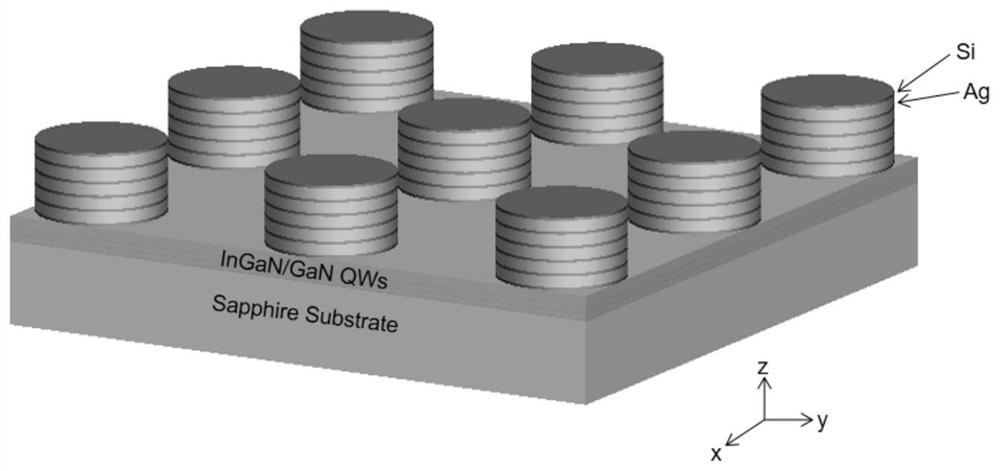
[0038] figure 1 It is a schematic diagram of an LED structure based on a patterned substrate of the present invention. As shown in the figure, the structure of the present invention from bottom to top includes a sapphire substrate with a thickness of 100nm, and three layers of InGaN / GaN layers are superimposed on the sapphire substrate, wherein each layer of InGaN / GaN layer consists of a 2nm thick InGaN layer and a 10nm-thick GaN layer on the upper layer; then a 10nm-thick GaN barrier layer is stacked on the uppermost GaN layer; and then 5 layers of Ag / Si layers are stacked on the barrier layer, wherein each layer of Ag / Si The layer consists of a 3nm thick Si layer on the lower layer and a 20nm thick Ag layer on the upper layer; finally a 5nm Si layer is superimposed on top of the uppermost Ag layer as a surface protection layer.

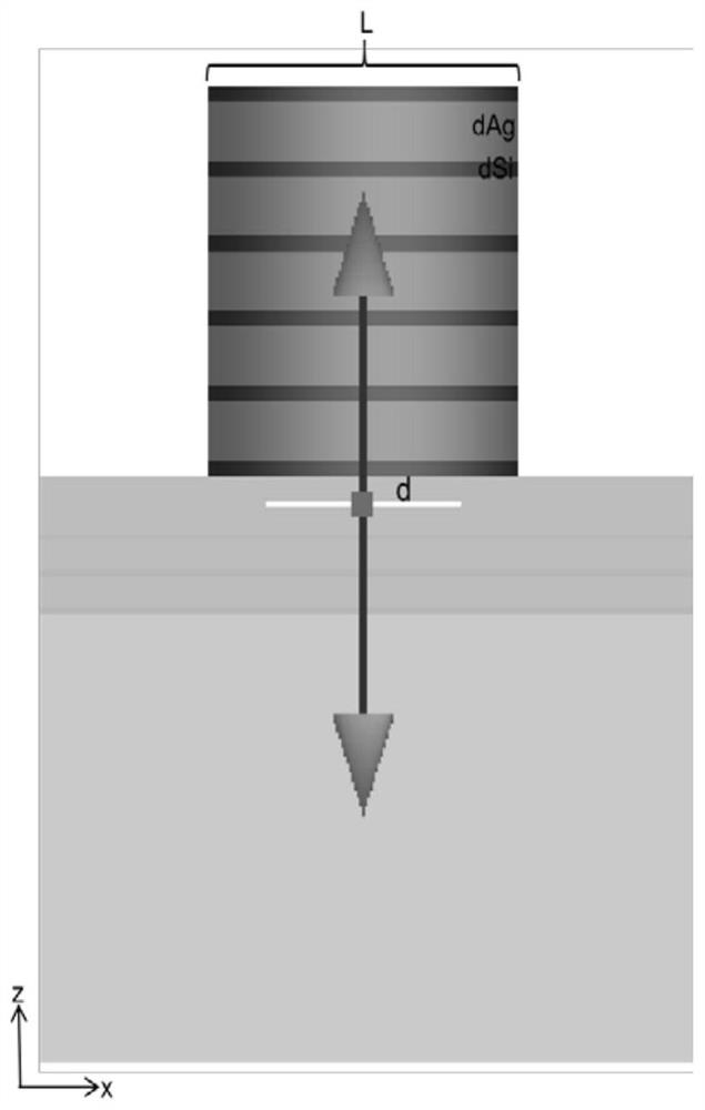
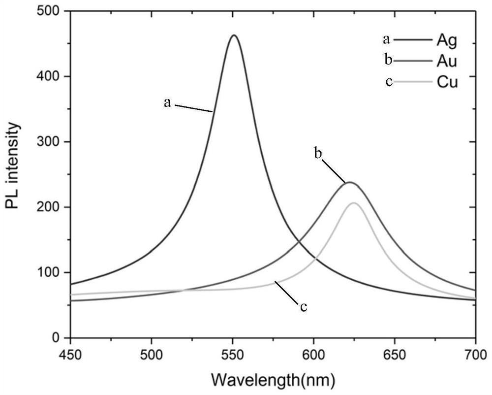
[0039] figure 2 It is a schematic diagram of the two-dimensional LED structure of the present invention. As the emission wavelength approaches ...


PUM

PropertyMeasurementUnit
thicknessaaaaaaaaaa
thicknessaaaaaaaaaa
thicknessaaaaaaaaaa

Abstract

The invention discloses an LED based on a patterned substrate and a preparation method thereof. The LED based on the patterned substrate structurally and sequentially comprises a sapphire substrate with two polished sides, three pairs of InGaN / GaN layer quantum wells, a barrier layer made of GaN, five pairs of Ag / Si layer hyperbolic metamaterials and a surface protection layer Si layer from bottomto top. On the basis of a traditional LED, a plurality of layers of hyperbolic metamaterials are added, so that the LED luminous efficiency of the patterned substrate reaches 180 times and is far higher than that of the traditional LED, and the LED is simple in technological process, low in cost, stable in processing technology and easy to produce in batches. Therefore, the LED and the preparation method a great application prospect in LED research.

Description

technical field [0001] The invention relates to the technical field of biosensors, in particular to an LED based on a patterned substrate and a preparation method thereof. Background technique [0002] Light-emitting diodes (LEDs) are called the fourth-generation light source, which has the characteristics of energy saving, environmental protection, safety, long life, low power consumption, low heat, high brightness, waterproof, miniature, shockproof, easy dimming, concentrated beam, and easy maintenance. With the continuous improvement of LED performance, LED has been widely used in various fields, such as automotive lamps, LCD backlights, lighting sources and so on. However, the luminous efficiency of LED is very low, which limits its development, so many researchers have been working hard to improve this problem. In recent years, the study of improving the emission efficiency of LEDs by using surface plasmon resonance (SPR) has attracted great interest because the lumino...

Claims


Application Information

Patent Timeline
Patent Type & Authority Applications(China)
IPC IPC(8): H01L33/06H01L33/44H01L33/00
CPCH01L33/007H01L33/06H01L33/44
Inventor 李卫冯烨赵建胜陈剑锋
Owner NANJING UNIV OF POSTS & TELECOMM
Why Eureka
Try Eureka