Anti-electromagnetic radiation ultrathin film, device, preparation method and application

An anti-electromagnetic radiation, ultra-thin film technology, applied in sputtering coating, electrical components, magnetic field/electric field shielding, etc., can solve the problem of low transmittance in the visible light band, inability to realize ultra-broadband electromagnetic shielding, complex structure and manufacturing process and other problems, to achieve the effect of excellent electromagnetic shielding effect, simple structure and easy processing

Pending Publication Date: 2020-11-20
SHANDONG UNIV
View PDF8 Cites 6 Cited by
  • Summary
  • Abstract
  • Description
  • Claims
  • Application Information

AI Technical Summary

Problems solved by technology

Neither of these two transparent radiation-proof films can achieve ultra-broadband electromagnetic shielding, and

Method used


Image

  • Anti-electromagnetic radiation ultrathin film, device, preparation method and application
  • Anti-electromagnetic radiation ultrathin film, device, preparation method and application
  • Anti-electromagnetic radiation ultrathin film, device, preparation method and application

Examples


preparation example Construction

[0038] In a third aspect, the present invention provides a method for preparing the above-mentioned ultra-thin film for preventing electromagnetic radiation, comprising the steps of:

[0039] It is prepared by electron beam evaporation coating technology or magnetron sputtering technology.

[0040] In a fourth aspect, the present invention provides the application of the above-mentioned ultra-thin film for preventing electromagnetic radiation in observation windows of microwave anechoic chambers and electromagnetic compatibility rooms, or application in protective glass of secret rooms.

Embodiment 1

[0042] An ultra-thin film with high transmittance in the visible light band and high shielding property in the microwave band is prepared by using titanium oxide and metal silver.

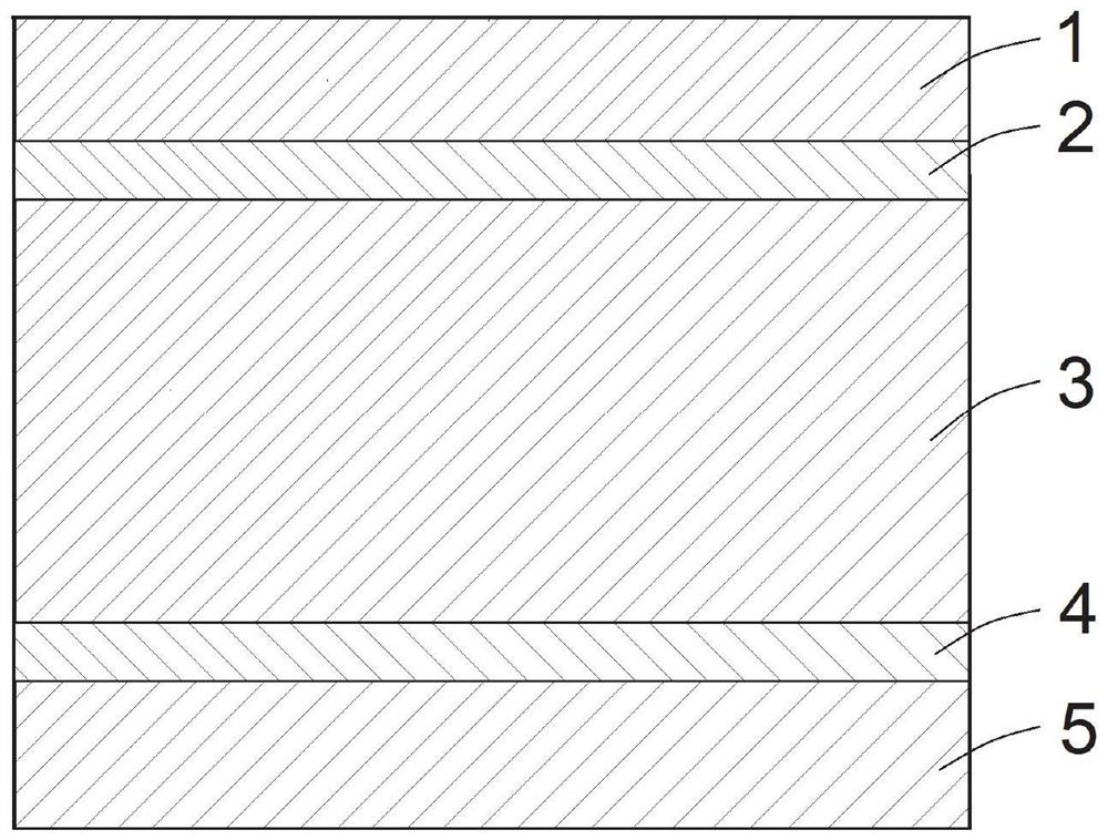
[0043] Such as figure 1 As shown, the first dielectric layer of the ultra-thin film is a 40nm titanium oxide layer, the first metal layer is a 12nm silver layer, the second dielectric layer is an 80nm titanium oxide layer, and the second metal layer is a 12nm silver layer. The third dielectric layer is a 40nm titanium oxide layer.

[0044] The ultra-thin film is integrally prepared on a glass substrate with a refractive index of 1.52 by electron beam evaporation process.

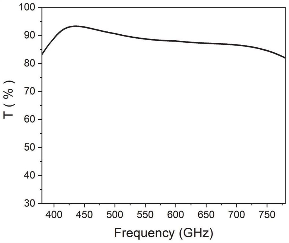
[0045] figure 2 Because of the transmission spectrum of the ultra-thin film in the visible light band, in the wavelength range of the visible light range (380-780nm), the transmittance exceeds 80%.

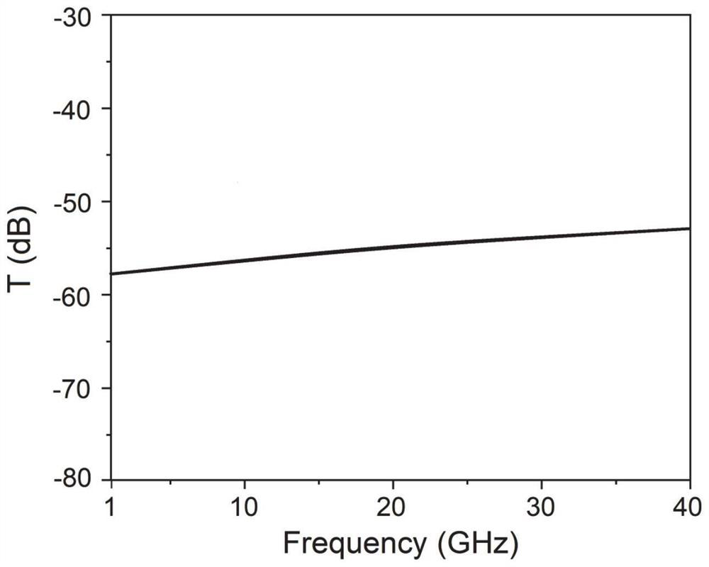
[0046] image 3 Because of the transmission spectrum of the ultra-thin film in the microwave section, the electromagnetic shie...

Embodiment 2

[0048] An ultra-thin film with high transmittance in the visible light band and high shielding property in the microwave band is prepared by using silicon oxide and metal silver.

[0049] The first dielectric layer of the ultra-thin film is a 50nm silicon oxide layer, the first metal layer is a 15nm gold layer, the second dielectric layer is a 100nm silicon oxide layer, the second metal layer is a 15nm gold layer, and the third dielectric layer is a 15nm gold layer. The layer is a 50nm silicon oxide layer.


PUM

PropertyMeasurementUnit
Thicknessaaaaaaaaaa
Thicknessaaaaaaaaaa

Abstract

The invention discloses an anti-electromagnetic radiation ultrathin film, a device, a preparation method and application, and the ultrathin film is of a laminated structure and is sequentially provided with a first dielectric layer, a first metal layer, a second dielectric layer, a second metal layer and a third dielectric layer. The dielectric layer is made of a visible light band transparent dielectric material; the first dielectric layer and the third dielectric layer are the same in thickness and are both smaller than the second dielectric layer in thickness. The anti-electromagnetic radiation ultrathin film is high in transparency in a visible light band, and the transmittance in the visible light band is greater than 80%. An alternate film layer structure composed of metal and a medium is utilized, and multiple reflection of light waves in a multilayer film is utilized, so that enhanced transmission in a visible light wave band is realized. 1G-40GHz ultra-wideband electromagneticshielding can be realized, the shielding effect is good, and the electromagnetic shielding effect is superior to 50dB.

Description

technical field [0001] The invention belongs to the technical field of anti-electromagnetic radiation films, and in particular relates to an anti-electromagnetic radiation ultra-thin film, a device, a preparation method and an application. Background technique [0002] The information disclosed in this background section is only intended to increase the understanding of the general background of the present invention, and is not necessarily taken as an acknowledgment or any form of suggestion that the information constitutes the prior art already known to those skilled in the art. [0003] With the continuous development of modern wireless communication technology, especially the large-scale use of 5G technology, it has brought great convenience to human beings. The development trend of the new generation of communication technology is to gradually advance the frequency of electromagnetic waves used to higher frequencies with greater load information, which makes the frequen...

Claims


Application Information

Patent Timeline
IPC IPC(8): H05K9/00C23C14/08C23C14/10C23C14/18C23C14/20C23C14/30C23C14/35C03C17/36
CPCH05K9/0088C23C14/185C23C14/205C23C14/20C23C14/18C23C14/086C23C14/081C23C14/083C23C14/10C23C14/08C23C14/30C23C14/352C03C17/36C03C17/3639C03C17/3644C03C17/3649C03C17/3676
Inventor 路光严发宝苏艳蕊陈耀武昭
Owner SHANDONG UNIV
Why Eureka
Try Eureka