Silicon-based on-chip Fourier transform spectrometer with high resolution and large measurement range

A technology of Fourier transform and measurement range, which is applied in the field of high-performance Fourier transform spectrometers, can solve the problems of large size, difficult measurement range, high crosstalk waveguide, etc., achieve high signal-to-noise ratio, increase the measurement range, The effect of reducing the number

Active Publication Date: 2020-12-01
ZHEJIANG UNIV
View PDF7 Cites 3 Cited by
  • Summary
  • Abstract
  • Description
  • Claims
  • Application Information

AI Technical Summary

Problems solved by technology

The solution using a dispersive spectrometer: Although this solution can achieve higher resolution, it is difficult to achieve high luminous flux due to the limitation of its physical mechanism
For the currently commonly used on-chip Fourier spectrometers, such as spatial extrapolation spectroscopy (SHS), although extremely high resolution can be achieved, the requirements of the Mach-Zehnder array make its size huge, and it is difficult to achieve large measurements. scope
For the newly proposed digital Fourier transform spectrometer, although higher resolution and larger bandwidth can be achieved, when its performance is to be further improved, it will face the problem of crosstalk caused by the increase in the number of optical switches and the increase in the length of the waveguide. The high waveguide loss problem of

Method used


Image

  • Silicon-based on-chip Fourier transform spectrometer with high resolution and large measurement range
  • Silicon-based on-chip Fourier transform spectrometer with high resolution and large measurement range
  • Silicon-based on-chip Fourier transform spectrometer with high resolution and large measurement range

Examples


specific Embodiment

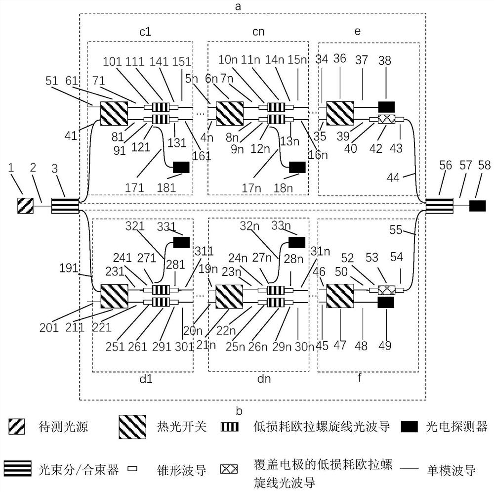
[0053] Here, N=2, M=10 is an example to provide a specific embodiment of the present invention, emphatically explain the on-off control relationship of each optical switch in the optical path selector of each level, the specific embodiment of the present invention is as follows:

[0054] The silicon nanowire optical waveguide based on silicon insulator (SOI) material is selected: the core layer is silicon material, the thickness is 220nm, and the refractive index is 3.4744; the lower cladding material is SiO 2 , with a thickness of 2 μm and a refractive index of 1.4404; the upper cladding material is SiO 2 , the thickness is 1.5 μm, and the refractive index is 1.4404; the metal material of the heating electrode is titanium gold.

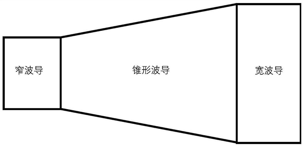
[0055] For a single-mode input waveguide 2, the width is 0.45 μm and the length is 100 μm. For the waveguide in the multi-stage optical path selector, the optical path selector cn of the upper interference arm a and the dn of the lower interference ...


PUM

PropertyMeasurementUnit
thicknessaaaaaaaaaa
thicknessaaaaaaaaaa
thicknessaaaaaaaaaa

Abstract

The invention discloses a silicon-based on-chip Fourier transform spectrometer with high resolution and a large measurement range. A to-be-measured light source is connected with an input waveguide; the output end of the input waveguide is connected with the input end of a 3dB power beam splitter; two ends of the 3dB beam splitter are respectively connected with one ends of multi-stage optical path selectors, and the two multi-stage optical path selectors are used as upper and lower interference arms; the output ends of the two multi-stage optical path selectors are connected with low-loss Euler spiral lines which have a specific length and is covered with metal electrodes; the other ends of the two low-loss spiral line waveguides are simultaneously input to the input end of the optical power beam combiner; and the output end of the optical power beam combiner is connected with the input end of the optical power detector to monitor the intensity of output optical signals. According tothe invention, the low-loss waveguide and the quasi-continuous thermal regulation waveguide are combined with a traditional on-chip Fourier spectrometer for the first time, and the silicon-based on-chip Fourier transform spectrometer can be used for biosensing, spectral measurement and other systems, and has the advantages of high resolution, large measurement range, high luminous flux, compact structure and the like.

Description

technical field [0001] The invention relates to an on-chip Fourier transform spectrometer, in particular to a high-performance Fourier transform spectrometer based on quasi-continuous adjustment for realizing high resolution and large measurement range. Background technique [0002] A spectrometer is a scientific instrument that decomposes the complex spectrum to be measured into spectral lines. Traditional spectrometers have disadvantages such as large volume, complex structure, and high price. With the continuous development of modern biology, medicine, aerospace, and environmental detection technologies, there is an increasing demand for micro-spectrometers that can monitor and sense the spectra of organisms and materials in real time. [0003] In terms of the performance requirements of the on-chip spectrometer, on the one hand, it has high requirements for high spectral resolution, which can meet the needs of modern sophisticated biological and environmental monitoring;...

Claims


Application Information

Patent Timeline
Patent Type & Authority Applications(China)
IPC IPC(8): G01J3/45G01J3/08G01J3/02
CPCG01J3/0205G01J3/0216G01J3/0237G01J3/0294G01J3/08G01J3/45
Inventor 戴道锌张龙
Owner ZHEJIANG UNIV
Why Eureka
Try Eureka