

A kind of gan-based lateral junction barrier Schottky diode and preparation method thereof
A junction-barrier Schottky and diode technology, applied in diodes, semiconductor/solid-state device manufacturing, semiconductor devices, etc., can solve the problem of difficult process, unable to fully utilize the advantages of junction-barrier Schottky diode structure, and vertical structure leakage large and other problems, to achieve the effects of suppressing the reduction effect, suppressing the control reverse leakage current, and low turn-on voltage
- Summary
- Abstract
- Description
- Claims
- Application Information
AI Technical Summary
Problems solved by technology
Method used
Image

Examples
Embodiment 1
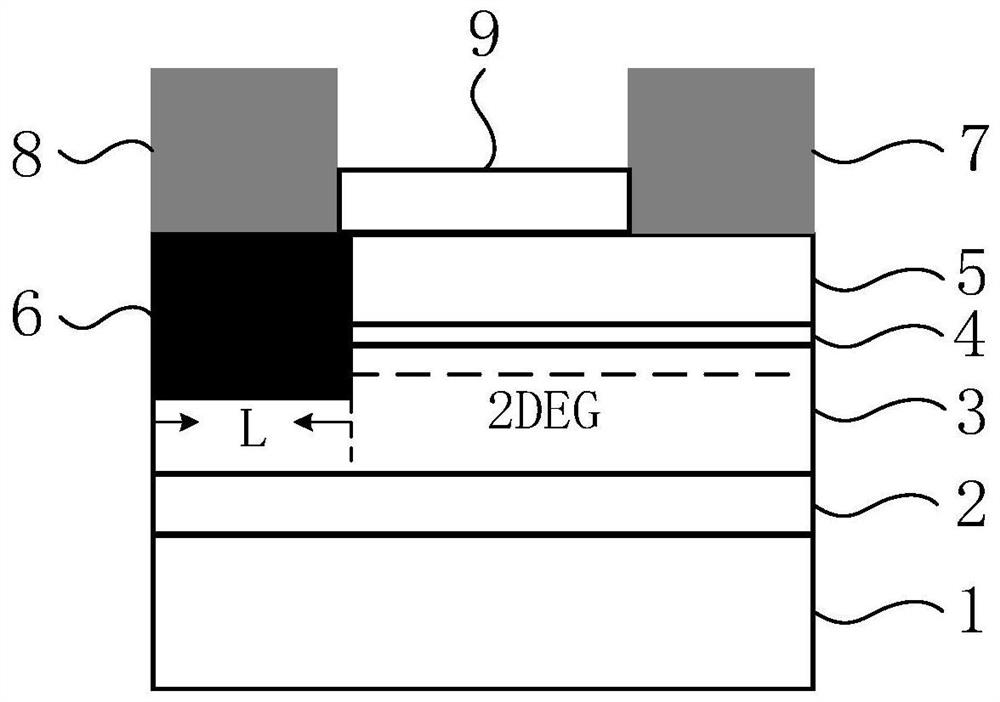
[0032] See figure 1 and Figure 4 , figure 1 A cross-sectional structural diagram of a Schottky diode based on a GaN lateral junction barrier provided in an embodiment of the present invention, Figure 4 This is a top view of a Schottky diode based on a GaN lateral junction barrier provided in an embodiment of the present invention. A GaN-based lateral junction barrier Schottky diode, comprising: a substrate layer 1, a nucleation layer 2, a buffer layer 3, an insertion layer 4, a barrier layer 5 and a passivation layer 9 that are sequentially stacked from bottom to top;
[0033] A P injection region 6 is disposed in the buffer layer 3, the insertion layer 4 and the barrier layer 5, and is located at one end of the buffer layer 3, the insertion layer 4 and the barrier layer 5, and the P injection region 6 includes several P regions and several N region, and each of the N regions is arranged between two adjacent P regions;
[0034] The anode electrode 8 is located on the upp...
Embodiment 2
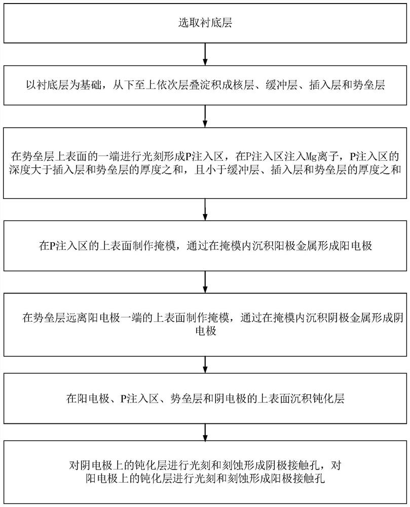
[0040] On the basis of Example 1, please refer to figure 2 and Figure 3a ~ Figure 3j , figure 2 A flow chart of a method for preparing a Schottky diode based on a GaN lateral junction barrier provided in an embodiment of the present invention, Figure 3a ~ Figure 3j A schematic diagram of a fabrication process of a Schottky diode based on a GaN lateral junction barrier provided in an embodiment of the present invention.
[0041]In this embodiment, the material of the substrate layer 1 is sapphire, the material of the nucleation layer is AlN, the material of the insertion layer 4 is AlN, and the material of the passivation layer 9 is SiN / SiO 2 .
[0042] A preparation method based on a GaN lateral junction barrier Schottky diode, comprising:
[0043] Step 1. Select the substrate layer 1.
[0044] The substrate layer 1 of sapphire material is selected.
[0045] Step 2: Based on the substrate layer 1, a nucleation layer 2, a buffer layer 3, an insertion layer 4 and a bar...
Embodiment 3
[0065] On the basis of Example 1, please refer to figure 2 and Figure 3a ~ Figure 3j , figure 2 A flow chart of a method for preparing a Schottky diode based on a GaN lateral junction barrier provided in an embodiment of the present invention, Figure 3a ~ Figure 3j A schematic diagram of a fabrication process of a Schottky diode based on a GaN lateral junction barrier provided in an embodiment of the present invention.
[0066] In this embodiment, the material of the substrate layer 1 is silicon carbide, the material of the insertion layer 4 is AlN, and the material of the passivation layer 9 is SiN / HfO 2 .
[0067] A preparation method based on a GaN lateral junction barrier Schottky diode, comprising:
[0068] Step 1. Select the substrate layer 1.
[0069] The substrate layer 1 of silicon carbide material is selected.
[0070] Step 2: Based on the substrate layer 1, a nucleation layer 2, a buffer layer 3, an insertion layer 4 and a barrier layer 5 are sequentially ...
PUM
| Property | Measurement | Unit |
|---|---|---|
| thickness | aaaaa | aaaaa |
| thickness | aaaaa | aaaaa |
| thickness | aaaaa | aaaaa |
Abstract
Description
Claims
Application Information