Perovskite polycrystalline sheet and preparation method and application thereof

A technology of perovskite and perovskite precursors, which is applied in the preparation of amino compounds from amines, semiconductor/solid-state device manufacturing, photovoltaic power generation, etc., and can solve the problems of lack of perovskite thick film preparation methods

Pending Publication Date: 2020-12-29
SHAANXI NORMAL UNIV
View PDF5 Cites 1 Cited by
  • Summary
  • Abstract
  • Description
  • Claims
  • Application Information

AI Technical Summary

Problems solved by technology

[0004] The purpose of the present invention is to overcome the above-mentioned shortcoming of the prior art, provide a kind of perovskite polycrystalline sheet and its preparation method and application, to solve the problem of lack of perovskite thick film preparation method in the prior art

Method used


Image

  • Perovskite polycrystalline sheet and preparation method and application thereof
  • Perovskite polycrystalline sheet and preparation method and application thereof
  • Perovskite polycrystalline sheet and preparation method and application thereof

Examples


Embodiment 1

[0039] 1. Add 1g of CH 2 NH 3 Dissolve I powder in 10mL of isopropanol, stir until dissolved at 80°C, then add 2g of PbI 2 The powder was poured into the solution, stirred for 2 hours, centrifuged three times to obtain solid perovskite powder, and dried at 60° C. for 12 hours to obtain perovskite powder.

[0040] 2. Put the perovskite powder into a circular mold, press high temperature and high pressure (10MPa, 150°C) for 5 hours, and then press the raw material into flakes to obtain perovskite polycrystalline flakes;

[0041] 3. Take out the cooled wafer, and vapor-deposit gold with a thickness of 50nm and 100nm on both sides as electrodes;

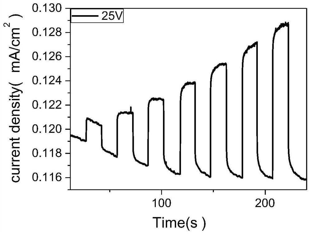
[0042] 4. Test the sensitivity of the prepared X-ray detector under different conditions.

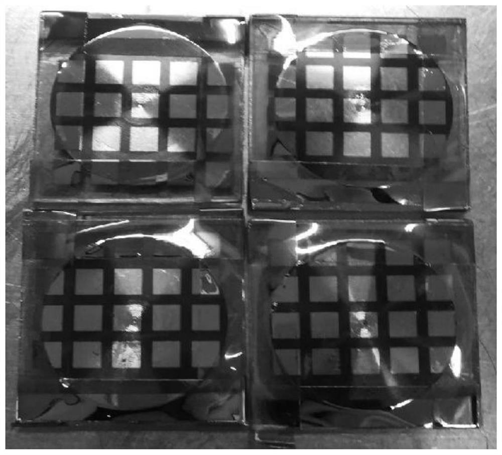
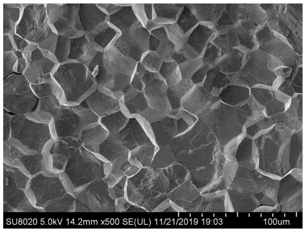
[0043] see figure 1 , do the X-ray detector for the perovskite multi-chip prepared in this embodiment, see figure 2 Make the metallographic diagram of the perovskite polycrystalline flake for this embodiment, as can be seen from the figure, th...

Embodiment 2

[0045] 1. Add 1g of CH 2 NH 3 Dissolve Br powder in 10mL of isopropanol, stir until dissolved at 80°C, then add 2g of PbBr 2 The powder was poured into the solution, stirred for 2 hours, centrifuged three times, and dried at 80° C. for 12 hours to obtain the perovskite powder.

[0046] 2. Put the perovskite powder into a circular mold, press high temperature and high pressure (10MPa, 150°C) for 8 hours, and then press the raw material into flakes to obtain perovskite polycrystalline flakes;

[0047] 3. Take out the cooled wafer, spin-coat an electron transport layer (20mg / mL PCBM solution) on one side, and leave the other side untreated;

[0048] 4. Take out the spin-coated wafer, and vapor-deposit gold with a thickness of 50nm and 100nm on both sides as electrodes;

[0049] 5. Test the sensitivity of the prepared X-ray detector under different conditions.

Embodiment 3

[0051] 1. Dissolve 1.5g of CsBr powder in 10mL of isopropanol, stir until dissolved at 80°C, then dissolve 2g of PbBr 2 The powder was poured into the solution, stirred for 2 hours, centrifuged three times, and dried at 100° C. for 12 hours to obtain the perovskite powder.

[0052] 2. Put the perovskite powder into a circular mold, and press the raw material into flakes by means of high temperature and high pressure (10MPa, 150°C, 1h) to obtain perovskite polycrystalline flakes;

[0053] 3. Take out the cooled wafer, and spin-coat electron transport layers (20 mg / mL PCBM solution) on both sides of the wafer;

[0054] 4. Take out the spin-coated wafer, and vapor-deposit gold with a thickness of 50nm and 100nm on both sides as electrodes;

[0055] 5. Test the sensitivity of the prepared X-ray detector under different conditions.


PUM

PropertyMeasurementUnit
Sizeaaaaaaaaaa
Sensitivityaaaaaaaaaa

Abstract

The invention discloses a perovskite polycrystalline sheet and a preparation method and application thereof. The preparation method includes the steps: by means of a solution method, AX powder is dissolved in an organic solvent through a solution compatible with the AX powder, then PbX2 powder is added into the solution, and the PbX2 powder and the AX powder can react to generate a perovskite precursor; and the generated perovskite precursor is insoluble in the organic solvent, so that the perovskite precursor can be separated from a process solution through a centrifugal process. The preparation process is different from an existing preparation process of an in-situ hot pressing method, the perovskite powder prepared through the solution method is more uniform in raw material, the precursor can be sufficiently reacted, the raw material utilization rate can be 80%, and raw material waste is avoided.

Description

【Technical field】 [0001] The invention belongs to the field of semiconductor optoelectronic materials, and in particular relates to a perovskite polycrystalline thin slice and a preparation method and application thereof. 【Background technique】 [0002] Lead halide perovskite materials have excellent photoelectric properties and are widely used in solar cells, LEDs, lasers, ray detectors and other devices. At present, it has been found that perovskite materials have high sensitivity as radiation detectors, and have received widespread attention. However, most of the high-performance devices reported so far are single crystals with small areas. In order to further realize the large-scale application of perovskite materials, the development of preparation technologies for large-area perovskite materials has become a problem that needs to be solved in current research. At the same time, the performance of perovskite ray detectors is positively correlated with the thickness of ...

Claims


Application Information

Patent Timeline
IPC IPC(8): C01G21/16H01L51/48H01L51/42C07C209/68C07C211/04
CPCC01G21/16C07C209/68C01P2002/72C01P2002/34C01P2004/03C01P2006/40H10K71/12H10K30/00C07C211/04Y02E10/549
Inventor 刘生忠杨周贾珊珊肖英锐胡明昕刘渝城张云霞步诺莫莉红
Owner SHAANXI NORMAL UNIV
Why Eureka
Try Eureka