High-density low-crosstalk waveguide array based on micro-nano isolation structure

A technology of isolation structure and waveguide array, applied in the directions of light guides, instruments, optics, etc., can solve the problems of low emission efficiency and insufficient use of light, and achieve the effect of high product yield, transmittance and small size.

Active Publication Date: 2021-01-05
UNIV OF SHANGHAI FOR SCI & TECH
View PDF7 Cites 2 Cited by
  • Summary
  • Abstract
  • Description
  • Claims
  • Application Information

AI Technical Summary

Problems solved by technology

Most of the optical antennas in lidar are second-order gratings directly etched on the array waveguide, which makes the emission efficiency very low, and due to the existence of side lobes and grating lobes, most of the light energy cannot be fully utilized

Method used


Image

  • High-density low-crosstalk waveguide array based on micro-nano isolation structure
  • High-density low-crosstalk waveguide array based on micro-nano isolation structure
  • High-density low-crosstalk waveguide array based on micro-nano isolation structure

Examples


Embodiment Construction

[0023] In order to make the purpose, technical solution and advantages of the present invention clearer, the technical solution of the present invention will be further described below.

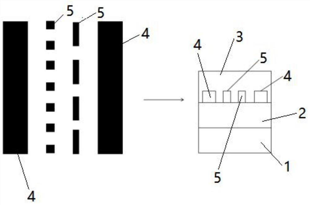
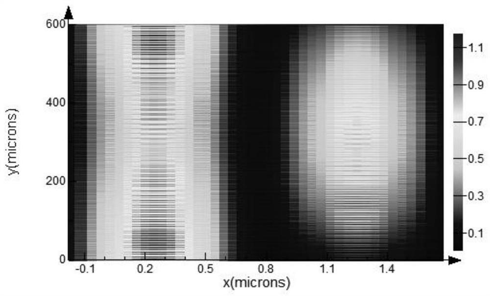
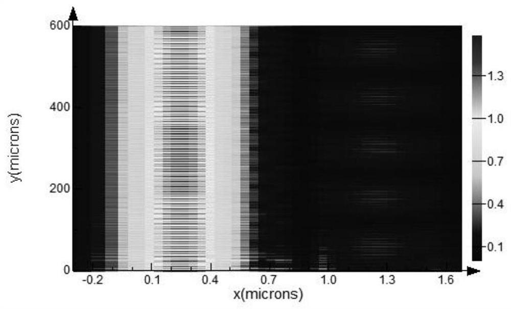
[0024] For wide waveguide designs, a large amount of coupling occurs in the straight waveguide coupling region. When designing this embodiment, if figure 1 As shown, the straight-width waveguide length is selected as 600 μm, the waveguide gap is 1 μm, and the waveguide width is 0.5 μm.

[0025] For the design of the periodic grating, two grating structures with different periods and duty ratios are added between the straight waveguides to achieve the effect of suppressing waveguide coupling. The first periodic grating structure in the middle of the wide waveguide is selected, with a period of 0.3-0.4 μm. The duty ratio is 0.3-0.4, the width is 0.12 μm, and the number of gratings is 1500-2000. The second grating structure has a period of 0.3-0.4 μm, a duty ratio of 0.5-0.8, a width of 0.12 μ...


PUM


Abstract

The invention provides a high-density low-crosstalk waveguide array based on a micro-nano isolation structure. The high-density low-crosstalk waveguide array comprises a substrate and a core layer based on a silicon waveguide, the core layer comprises two silicon wide waveguides with the same structural parameters and two silicon periodic gratings; and the two silicon wide waveguides are arrangedon the substrate, and two silicon periodic gratings with different parameter structures are arranged between the two adjacent silicon wide waveguides. Through the middle grating structure, phase mismatch of light between the different waveguides is achieved, and the effect of restraining coupling is achieved, so the provided waveguide array is compact in structure, high in transmittance and low incrosstalk.

Description

technical field [0001] The invention relates to the field of chip technology, in particular to a high-density and low-crosstalk waveguide array based on a micro-nano isolation structure. Background technique [0002] With the advent of the era of big data, the development of modern photonic technology has higher and higher requirements for device integration, on-chip device density, function, and performance. At the same time, silicon-on-insulator (SOI) material, as a hotspot material in optical integration research, is selected for its advantages of good light-guiding properties, strong light confinement and full compatibility with standard complementary metal-oxide-semiconductor (CMOS) processes. [0003] Chip-scale optical phased arrays enable small beam steering and lidar for unmanned aerial vehicles, precision robotics, and free-space optical communications. Since these applications require wide-angle beam steering and high optical power in the output beam, the natural...

Claims


Application Information

Patent Timeline
Patent Type & Authority Applications(China)
IPC IPC(8): G02B6/124
CPCG02B6/124
Inventor 冯吉军刘海鹏孙福领曾和平
Owner UNIV OF SHANGHAI FOR SCI & TECH
Why Eureka
Try Eureka