Micro light-emitting diode epitaxial structure and preparation method thereof

An epitaxial structure, light-emitting area technology, applied in the direction of final product manufacturing, sustainable manufacturing/processing, climate sustainability, etc., can solve the problem of unstable photoelectric conversion efficiency, decreased photoelectric conversion efficiency, low current density that cannot be applied to epitaxial wafers, etc. It can improve the radiative recombination efficiency and photoelectric conversion efficiency of carriers, reduce the defect density, and improve the carrier transport and recombination behavior.

Active Publication Date: 2021-01-08
TIANJIN SANAN OPTOELECTRONICS
View PDF4 Cites 1 Cited by
  • Summary
  • Abstract
  • Description
  • Claims
  • Application Information

AI Technical Summary

Problems solved by technology

Conventional epitaxial structure at less than 1A / cm 2 Under the current density, the photoelectric conversion efficiency is in a very unstable range. With the small change of the current, the photoelectric conversion efficiency will also drop sharply, which makes the traditional epitaxial wafers unable to be applied to products with low current density requirements.

Method used


Image

  • Micro light-emitting diode epitaxial structure and preparation method thereof
  • Micro light-emitting diode epitaxial structure and preparation method thereof
  • Micro light-emitting diode epitaxial structure and preparation method thereof

Examples


Embodiment 1

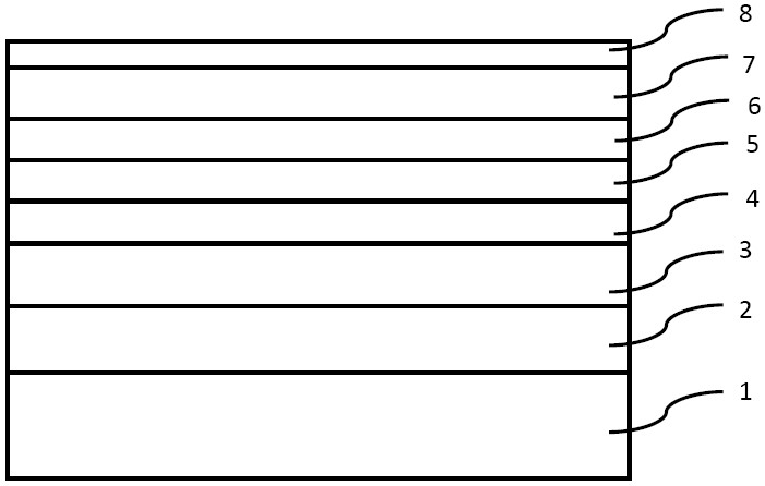
[0056] Please refer to Figure 1~Figure 5 , based on the purpose of the present invention, this embodiment provides a micro-LED epitaxial structure and a manufacturing method thereof, including the following process steps:

[0057] (1) Provide a substrate 1, which can be sapphire (Al 2 o 3 ), AlN or SiNx-plated sapphire (Al 2 o 3 ), Ga 2 o 3 , AlN or SiNxGa plating 2 o 3 , SiC, GaN, ZnO, Si or Ge at least one, this embodiment is preferably coated with AlN sapphire substrate.

[0058] (2) Epitaxial growth of the nucleation layer on the substrate 1 (not shown in the figure): AlGaN material is preferred, and the epitaxial growth method can be MOCVD (metal organic chemical vapor deposition) method, MBE (molecular beam epitaxy) method, CVD ( Chemical Vapor Deposition) method, HVPE (Hydride Vapor Phase Epitaxy) method, PECVD (Plasma Enhanced Chemical Vapor Deposition) method, preferably MOCVD, but the embodiment is not limited thereto. Put the AlN-coated sapphire substrate ...

Embodiment 2

[0069] In this embodiment, an alternative implementation is provided, which is specifically provided as follows.

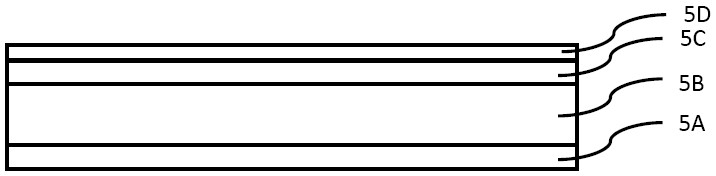
[0070] The description of the light-emitting area is as follows: the difference from the first embodiment is as follows, this embodiment is a multi-well layer design, as follows:

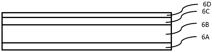
[0071] The first luminous area: can refer to Image 6 . After the growth of the third barrier layer 5C is completed, the first well layer 52D begins to grow during the process of cooling down to the temperature of the well layer (700~800°C), and the TMIN 1000sccm is injected, the material is InGaN, the rate is about 0.6 Å / s, and the thickness About 3~8 angstroms. After the growth of the first well layer is completed, the second well layer 52E is grown, the material is InGaN, the rate is about 0.3 angstroms / s, and the thickness is about 5~15 angstroms. After the growth of the second well layer is completed, When the temperature is raised to the barrier layer temperature (800-900° C.), ...

Embodiment 3

[0076] In this embodiment, an alternative implementation is provided, which is specifically provided as follows. The difference from the first embodiment is that the composite light emitting area is a combination of the first light emitting area and the second light emitting area.


PUM

PropertyMeasurementUnit
thicknessaaaaaaaaaa
thicknessaaaaaaaaaa
temperatureaaaaaaaaaa

Abstract

The invention provides a micro LED epitaxial structure. The epitaxial structure at least comprises an N-type layer, a light-emitting layer and a P-type layer. Wherein the light-emitting layer comprises quantum well structures of n periods, the quantum well structure of each period comprises a well layer and a barrier layer, the quantum well structure of n1 periods is defined as a first light-emitting region, the quantum well structure of n2 periods is defined as a second light-emitting region, n1 and n2 are greater than or equal to 1, n1 + n2 is less than or equal to n, and the first light-emitting region is closer to the N-type layer. The average band gap of the barrier layer materials of the two groups of light-emitting regions meets the following conditions: the first light-emitting region is smaller than the second light-emitting region; the average band gap of the well layer materials of the two groups of light-emitting regions satisfies the following condition: the first light-emitting region is greater than or equal to the second light-emitting region. According to the micro LED prepared by the epitaxial structure, the current density corresponding to the peak photoelectricconversion efficiency can be lower than 1A/cm<2>, and the photoelectric conversion efficiency is improved by about 30%.

Description

technical field [0001] The invention relates to a micro LED light-emitting element, which belongs to the technical field of semiconductor optoelectronics. Background technique [0002] The peak photoelectric conversion efficiency distribution of traditional epitaxial structure LEDs is greater than 5A / cm 2 The range of current density, such as Figure 9 As shown, most of the existing applications work at high current density (greater than 10A / cm 2 )area. However, the current used by Micro LEDs used in mobile phones (or watches, bracelets) is very small, often at the level of nA, converted into current density, at 0.1~1A / cm 2 between. Conventional epitaxial structure at less than 1A / cm 2 Under the current density, its photoelectric conversion efficiency is in a very unstable range. With the slight change of the current, the photoelectric conversion efficiency will also drop sharply, which makes the traditional epitaxial wafer unable to be applied to products with low curre...

Claims


Application Information

Patent Timeline
Patent Type & Authority Applications(China)
IPC IPC(8): H01L33/06H01L33/00H01L33/12H01L33/14H01L33/32
CPCH01L33/007H01L33/06H01L33/12H01L33/145H01L33/325C30B25/02C30B29/403Y02P70/50H01L33/32H01L33/08H01L33/025H01L27/156H01L33/0075H01L2933/0008
Inventor 李水清杜伟华赖昭序邓和清
Owner TIANJIN SANAN OPTOELECTRONICS
Why Eureka
Try Eureka