
Low-inductance silicon carbide module

A technology of silicon carbide and low inductance, applied in circuits, electrical components, electric solid devices, etc., can solve the problems of reducing the overall reliability of the module, increasing the turn-off loss of the chip, and the large inductance of the packaging loop, so as to improve the current output capability And the effect of service life, increased mutual inductance, and large cross-sectional area

Pending Publication Date: 2021-01-26
MACMIC SCIENCE & TECHNOLOGY CO LTD
View PDF0 Cites 0 Cited by
  • Summary
  • Abstract
  • Description
  • Claims
  • Application Information

AI Technical Summary

Problems solved by technology

[0003] The invention solves the problems in the related art that the silicon carbide semiconductor module package loop inductance is relatively large, and the existence of stray inductance will cause the increase of chip turn-off loss and overvoltage, thereby reducing the overall reliability of the module, and proposes a low inductance The silicon carbide module can improve the overcurrent capacity and thermal conductivity of the connected device; the metal connection block has a large cross-sectional area, which is not easy to deform under the action of external force, increasing reliability; reducing the inductance of the module, improving the current output capability and service life of the module

Method used


Image

  • Low-inductance silicon carbide module
  • Low-inductance silicon carbide module
  • Low-inductance silicon carbide module

Examples


Embodiment Construction

[0015] The following will clearly and completely describe the technical solutions in the embodiments of the present invention with reference to the accompanying drawings in the embodiments of the present invention. Obviously, the described embodiments are only some, not all, embodiments of the present invention. The following description of at least one exemplary embodiment is merely illustrative in nature and in no way taken as limiting the invention, its application or uses. Based on the embodiments of the present invention, all other embodiments obtained by persons of ordinary skill in the art without creative efforts fall within the protection scope of the present invention.

[0016] It should be noted that the terminology used here is only for describing specific implementations, and is not intended to limit the exemplary implementations according to the present application. As used herein, unless the context clearly dictates otherwise, the singular is intended to include...


PUM


Abstract

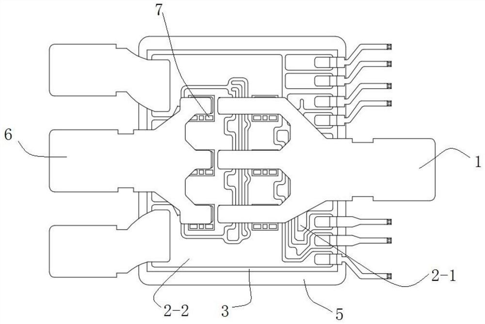
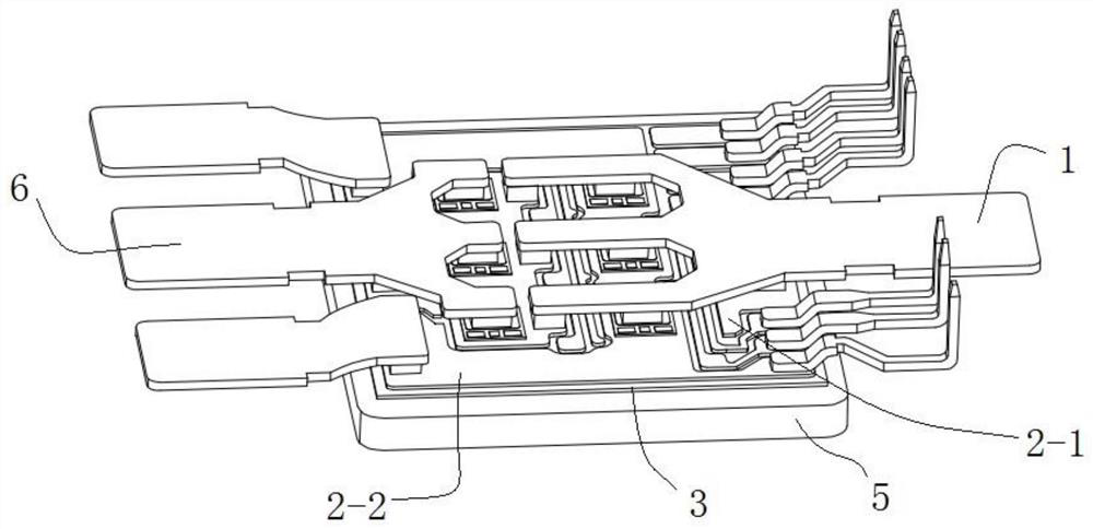
The invention relates to the technical field of silicon carbide semiconductor modules, in particular to a low-inductance silicon carbide module. The module comprises a current input terminal, a firstceramic copper-clad plate, a ceramic chip, a second ceramic copper-clad plate, a heat dissipation bottom plate, a current output terminal, a chip and a metal connecting block; the current input terminal and the current output terminal are parallel to the first ceramic copper-clad plate and are supported by the metal connecting block, and the chip is welded between the first ceramic copper-clad plate and the metal connecting block and is bonded with the current input terminal and the current output terminal through the metal connecting block; the ceramic chip is welded to the back face of the first ceramic copper-clad plate and connected with the second ceramic copper-clad plate, and the second ceramic copper-clad plate is connected with the heat dissipation bottom plate. According to the invention, the over-current capability and the heat conduction capability of the connecting device can be improved; the metal connecting block is large in cross sectional area and not prone to deformation under the action of external force, and reliability is improved; the inductance of the module is reduced, and current output capability and service life of the module are improved.

Description

technical field [0001] The invention relates to the technical field of silicon carbide semiconductor modules, in particular to a low-inductance silicon carbide module. Background technique [0002] The power semiconductor module is a combination according to certain functions and modes. The power semiconductor module is a combination of high-power electronic power devices according to certain functions and then potted into one. The power semiconductor module can realize different functions according to the different packaged components. The power semiconductor module can be used as an air-cooled module when equipped with air-cooled heat dissipation, and can be used as a water-cooled module when equipped with water-cooled heat dissipation. Silicon carbide semiconductors are widely used due to their higher operating temperature, higher breakdown voltage strength, higher thermal conductivity, and higher switching frequency. However, the existing silicon carbide semiconductor m...

Claims


Application Information

Patent Timeline
Patent Type & Authority Applications(China)
IPC IPC(8): H01L23/14H01L23/488H01L23/367H01L23/522H01L21/04
CPCH01L23/14H01L23/488H01L23/367H01L23/5227H01L21/0445H01L2224/40139
Inventor 石彩云张海泉麻长胜赵善麒
Owner MACMIC SCIENCE & TECHNOLOGY CO LTD
Learn More