
DNA sequencing device, solid-state nanopore array and preparation method of solid-state nanopore array

A DNA sequencing and nanopore array technology, applied in biochemical equipment and methods, nanotechnology, nanotechnology, etc., can solve the problems of affecting detection stability, inconvenient transportation and installation, and low recognition rate of base detection.

Pending Publication Date: 2021-02-02
SHENZHEN RUHAN GENE SCI & TECH LTD
View PDF0 Cites 1 Cited by
  • Summary
  • Abstract
  • Description
  • Claims
  • Application Information

AI Technical Summary

Problems solved by technology

[0005] First of all, the traditional method of manufacturing solid-state nanopore arrays is usually directly fabricated on silicon materials, and the nanopore channel length of silicon materials is too long, reaching more than 5nm. When multiple bases pass through in sequence, the sequencing current changes too long.
[0006] Secondly, due to the method of using external electrodes, the traditional method of manufacturing solid-state nanopore array DNA sequencing electrodes is relatively complicated and has disadvantages such as affecting detection stability, inconvenient transportation and installation, and increasing costs.
[0007] Thirdly, traditional solid-state nanopore array DNA sequencing devices can usually only test the same gene sequence at a time
[0008] Finally, the traditional solid-state nanopore array DNA sequencing device generally has the problem of low base detection and recognition rate due to the fast flow rate of DNA through the nanopore

Method used


Image

  • DNA sequencing device, solid-state nanopore array and preparation method of solid-state nanopore array
  • DNA sequencing device, solid-state nanopore array and preparation method of solid-state nanopore array
  • DNA sequencing device, solid-state nanopore array and preparation method of solid-state nanopore array

Examples


Embodiment Construction

[0029] In order to make the technical problems, technical solutions and beneficial effects to be solved by the present invention clearer and clearer, the present invention will be further described in detail below in conjunction with the accompanying drawings and embodiments. It should be understood that the specific embodiments described here are only for explaining the present invention, and are not intended to limit the present invention.

[0030] In the following description, use of suffixes such as 'module', 'part' or 'unit' for denoting elements is only for facilitating description of the present invention and has no specific meaning by itself. Therefore, 'module', 'part' or 'unit' may be used in combination.

[0031] It should be noted that the terms "first" and "second" in the description and claims of the present invention and the above drawings are used to distinguish similar objects, but not necessarily used to describe a specific sequence or sequence.

[0032] In ...


PUM


Abstract

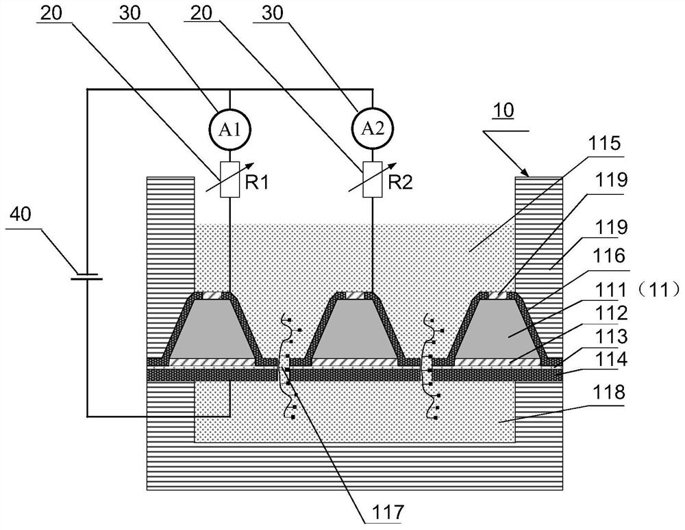
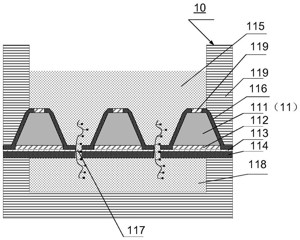
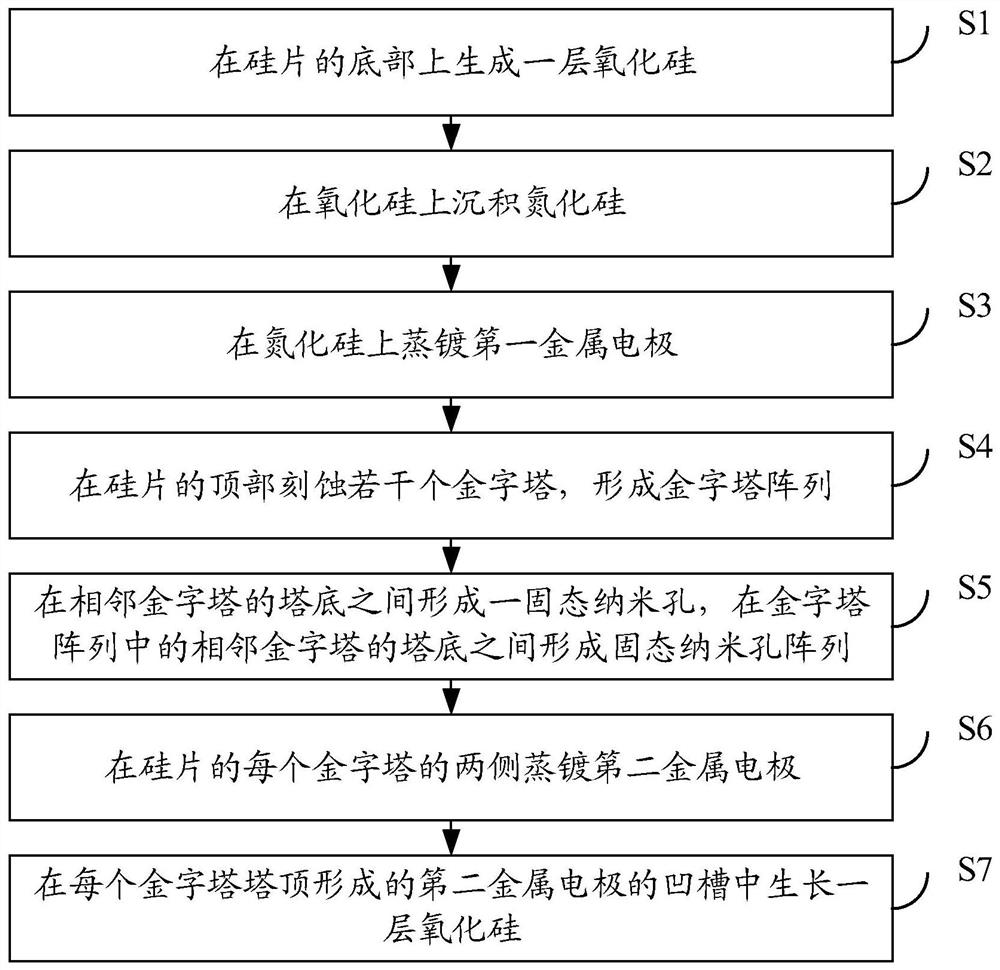
The invention discloses a DNA sequencing device, a solid-state nanopore array and a preparation method of the solid-state nanopore array. The solid-state nanopore array comprises a plurality of pyramids etched on a silicon wafer, silicon oxide grows below each pyramid, silicon nitride is deposited below the silicon oxide, and a first metal electrode is- evaporated below the silicon nitride; secondmetal electrodes are evaporated on the two sides of each pyramid, an inverted pyramid-shaped micro-cavity is formed between the second metal electrodes on the two sides of the adjacent pyramids, a solid-state nanopore is formed in the tower top of each inverted pyramid-shaped micro-cavity, and each solid-state nanopore forms a solid-state nanopore array; the first metal electrode, a variable resistor, a current measuring device, a power supply and the second metal electrodes form a plurality of longitudinal weak current measuring loops; and by adjusting the variable resistor, the current measuring device measures the longitudinal weak current of the longitudinal weak current measuring loops to sequence a DNA sequence passing through the solid-state nanopore array. According to the embodiment of the invention, the DNA sequencing precision and sequencing efficiency can be improved.

Description

technical field [0001] The invention relates to the field of gene detection, in particular to a DNA sequencing device, a solid-state nanopore array and a preparation method thereof. Background technique [0002] Since their introduction more than two decades ago, nanopore sensors have evolved into powerful tools for single-molecule studies. Moreover, due to its low cost, reliability, and rapid detection, nanopore sensors have become the most popular DNA (DeoxyriboNucleic Acid, deoxyribonucleic acid) sequencing method, which is expected to greatly increase the speed of gene sequencing and reduce the cost of gene sequencing. [0003] The single-hole solid-state nanopore DNA sequencing device can only test one DNA sequence at a time, and it is prone to congestion after multiple uses, thereby reducing the test efficiency. Therefore, the potential and application of porous solid-state nanopore array sensors have attracted more and more attention. [0004] However, traditional s...

Claims


Application Information

Patent Timeline
IPC IPC(8): C12M1/34C12M1/00C12Q1/6869B82Y15/00B82Y40/00
CPCC12Q1/6869B82Y15/00B82Y40/00C12Q2565/607C12Q2565/631
Inventor 莫晖周文益范建林张新联刘战隋国栋尹良超吴蒙卢大儒
Owner SHENZHEN RUHAN GENE SCI & TECH LTD
Learn More