Transparent conductive film, preparation method thereof, application and photoelectric device containing transparent conductive film

A technology of transparent conductive film and optoelectronic devices, which is applied in the manufacture of conductive/semiconductive layer equipment, electrical components, cable/conductor manufacturing, etc., and can solve problems such as difficult current flow, difficulty in applying optoelectronic products, and opaque conductive film

Pending Publication Date: 2021-02-02
SHANGHAI LANGYI FUNCTIONAL MATERIALS
View PDF1 Cites 1 Cited by
  • Summary
  • Abstract
  • Description
  • Claims
  • Application Information

AI Technical Summary

Problems solved by technology

[0008] The technical problem to be solved by the present invention is to overcome the conductive film in the prior art or the system is opaque, it is difficult to be suitable for optoelectronic products; ) transmission defects, and provide a transparent conductive film and its preparation method, application, optoelectronic device containing it

Method used


Image

  • Transparent conductive film, preparation method thereof, application and photoelectric device containing transparent conductive film
  • Transparent conductive film, preparation method thereof, application and photoelectric device containing transparent conductive film
  • Transparent conductive film, preparation method thereof, application and photoelectric device containing transparent conductive film

Examples


Embodiment 1

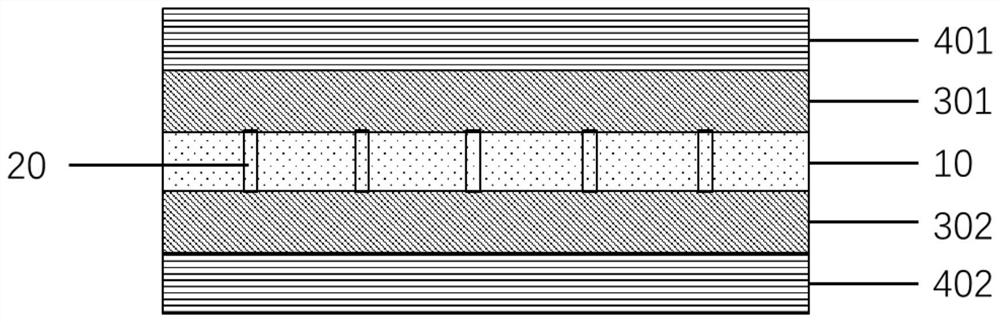
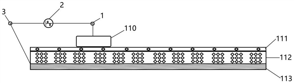
[0092] figure 1 It is a schematic cross-sectional structure diagram of the transparent conductive film of Example 1. The transparent conductive film successively includes: a first hardened layer 401, a first conductive film layer 301, a transparent substrate layer 10, a second conductive film layer 302, and a second hardened layer 401 stacked on each other, the transparent substrate layer Through holes 20 are distributed on 10 .

[0093] The preparation method of transparent conductive film is as follows:

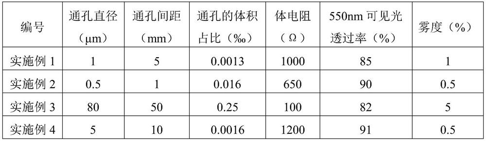
[0094] (1) First, the silver metal is embossed on the surface of the transparent PVC film 10, and the PVC film is pressed through to form a silver metal conductive channel 20 with a diameter of 1 μm, and the distance between the center points of two adjacent silver metal conductive channels is controlled to be 5mm. The volume ratio of the conductive channel to the transparent PVC film is 0.0013‰;

[0095] (2) Then, both sides of the PVC film are coated with silver nanowi...

Embodiment 2

[0098] The preparation method of transparent conductive film is as follows:

[0099] (1) First, use a laser puncher to prepare a through hole with a pore diameter of 0.5 μm on the surface of the transparent PC film, and control the distance between two adjacent holes and the center point of the hole to be 1mm, and the volume ratio of the through hole to the transparent PC film 0.016‰;

[0100] (2) then fill polypyrrole in hole;

[0101] (3) Finally, AZO was magnetron sputtered on both sides of the transparent PC film to prepare a transparent conductive layer.

Embodiment 3

[0103] The preparation method of transparent conductive film is as follows:

[0104] (1) First, copper metal is embossed on the surface of the transparent PI film, and the PI film is pressed through to form a copper metal conductive channel with a diameter of 80 μm. The distance between the center points of two adjacent copper metal conductive channels is controlled to be 50 mm, and the copper metal conductive channel The volume ratio of the transparent PI film is 0.25‰;

[0105] (2) Coating copper nanowires on one side of the PI film to prepare a transparent conductive layer, and magnetron sputtering AZO on the other side of the PI film to prepare a transparent conductive layer;

[0106] (3) Finally, a hardened layer of polyurethane is coated on the surface of the copper nanowires to prevent the copper nanowires from being stripped or oxidized.


PUM

PropertyMeasurementUnit
pore sizeaaaaaaaaaa
electrical resistanceaaaaaaaaaa
hazeaaaaaaaaaa

Abstract

The invention discloses a transparent conductive film, a preparation method thereof, application, and a photoelectric device containing the transparent conductive film. The transparent conductive filmsequentially comprises a first conductive film layer, a transparent substrate layer and a second conductive film layer which are overlapped with one another; a plurality of through holes are formed in the transparent substrate; the hole diameters of the through holes are 0.5-100 microns; when two or more through holes are formed in the transparent substrate, the distance between the center pointsof any two adjacent through holes ranges from 0.1 mm to 100 mm; the volume ratio of the through holes to the transparent substrate ranges from 0.0001% o to 2.5%; the through holes are filled with conducting media. According to the transparent conductive film, bulk phase conduction can be realized on the basis of not influencing the light transmittance of the material, the conductive performance is uniform, more signals can be generated, diversification of photoelectric products is realized, the erasable range of a conductive liquid crystal board can be controlled, the preparation process is simple, and industrial large-scale production is facilitated.

Description

technical field [0001] The invention relates to the field of optoelectronic products, in particular to a transparent conductive film, its preparation method, application, and an optoelectronic device containing the same. Background technique [0002] Optoelectronic products require the penetration of light and the conduction of electricity. Therefore, transparent conductive films are the basis of optoelectronic products. Optoelectronic products such as conductive liquid crystal panels, flat panel displays, touch panels, solar cells, electronic paper, and OLED lighting need to use transparent conductive film. [0003] The existing transparent conductive film is generally by magnetron sputtering ITO (indium tin oxide) layer on the surface of transparent film materials such as PET (polyethylene terephthalic acid), PC (polycarbonate) and PI (polyimide), In order to achieve the effect of surface conductivity. However, this kind of transparent conductive film can only achieve on...

Claims


Application Information

Patent Timeline
Patent Type & Authority Applications(China)
IPC IPC(8): H01B5/14H01B5/00H01B13/00G02F1/1333
CPCG02F1/1333H01B5/00H01B5/14H01B13/00H01B13/0026
Inventor 唐晓峰余子涯逯琪叶倩董建廷
Owner SHANGHAI LANGYI FUNCTIONAL MATERIALS
Why Eureka
Try Eureka