
Bit line driving structure and three-dimensional memory structure

A driving structure and driving device technology, which is applied in the direction of electric solid-state devices, semiconductor devices, electrical components, etc., and can solve problems such as the drop of withstand voltage value

Inactive Publication Date: 2021-02-05
YANGTZE MEMORY TECH CO LTD
View PDF7 Cites 0 Cited by
  • Summary
  • Abstract
  • Description
  • Claims
  • Application Information

AI Technical Summary

Problems solved by technology

Compared with the driving device located in the middle of the array with other driving devices on the left and right sides, the withstand voltage value of the driving device located at the edge of the array will drop significantly, making it the most likely to occur in the entire driving circuit array. Breakdown of Weak Links

Method used


Image

  • Bit line driving structure and three-dimensional memory structure
  • Bit line driving structure and three-dimensional memory structure
  • Bit line driving structure and three-dimensional memory structure

Examples


Embodiment 1

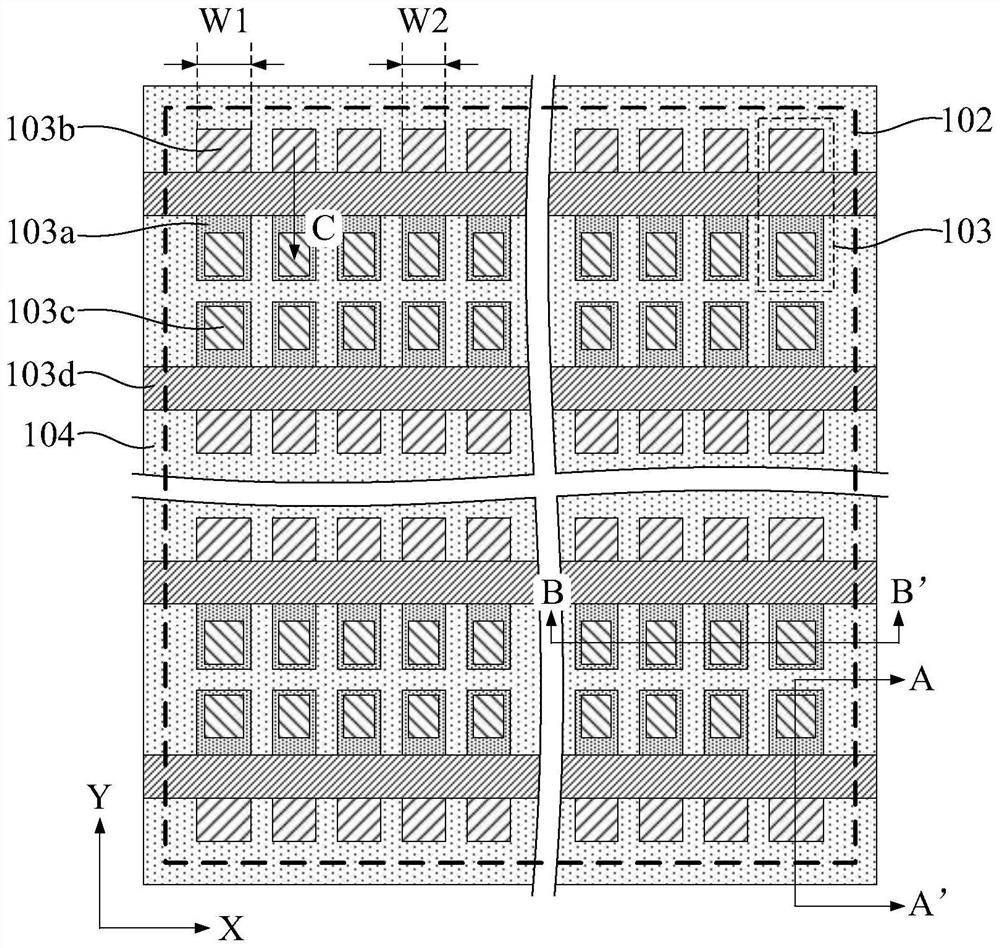
[0067] see Figure 1 to Figure 6 , this embodiment provides a bit line driving structure, characterized in that: comprising:

[0068] The first substrate 101 has a first surface and a second surface opposite to each other;

[0069] A driving device array 102 formed on the first surface side of the first substrate 101, the driving device array 102 is composed of a plurality of driving devices 103 arranged;

[0070] The driving device 103 includes an active device region 103a formed in the first substrate 101, a source region 103b and a drain region 103c formed in the active device region 103a, and an active device region 103c formed in the active device region 103a. The gate structure 103d above the region 103a; the source region 103b and the drain region 103c are respectively located on both sides of the gate structure 103d; there are intervals between the plurality of active device regions 103a;

[0071] The direction in which the source region 103b points to the drain regi...

Embodiment 2

[0085] see Figure 6 , this embodiment provides a three-dimensional memory structure, characterized in that it includes:

[0086] The driving structure for improving the withstand voltage value of the bit line driving circuit as described in the first embodiment;

[0087] a second substrate 106, which has a third surface and a fourth surface oppositely disposed;

[0088] A memory array structure formed on the third surface of the second substrate 106, the memory array structure comprising a plurality of memory strings 108 and a bit line structure 109 connecting the memory strings 108;

[0089] As in the bit line driving structure described in Embodiment 1, the bit line driving structure is connected to the bit line structure 109 .

[0090] As an example, there are multiple storage strings 108 formed in the stack structure 107 . The stack structure 107 includes alternately stacked gate layers 107a and isolation layers 107b, and a top selection gate 107c at the top and a bott...


PUM


Abstract

The invention provides a bit line driving structure and a three-dimensional memory structure. The bit line driving structure comprises: a first substrate; and a driving device array which is formed onone side of the first surface of the first substrate and is formed by arranging a plurality of driving devices, wherein the driving device comprises an active device region, a source region, a drainregion and a gate structure, the source region and the drain region are respectively positioned on two sides of the gate structure, gaps are formed among the active device regions, in the same row ofdriving devices arranged in the row direction, the widths of the source region and the drain region of the driving devices located on the edges of the two sides are larger than those of the source region and the drain region of the driving devices located on the edges of the non-two sides. According to the invention, a driving device with wider source and drain region widths in edge regions on twosides in the row direction is introduced, and the source and drain breakdown voltage of the device is improved by increasing the source and drain region widths in the edge regions, increasing the junction area of the device, broadening a depletion region and reducing an electric field; and by improving the weak point of voltage withstanding of the driving device array, the overall voltage withstanding performance of the driving device array is improved.

Description

technical field [0001] The invention relates to the field of semiconductor integrated circuit manufacturing, in particular to a bit line driving structure and a three-dimensional memory structure. Background technique [0002] As the capacity and number of layers of 3D NAND memory continue to increase, the operating voltage used to drive the memory also increases, and related circuits need to ensure that they work under higher voltage conditions without breakdown and other abnormalities. For example, in the erasing operation of some memory cells, the bit line driver circuit needs to withstand a high voltage of at least 23V, and as the device design requires that the threshold voltage distribution of array cells be more convergent, the voltage value will be further increased. [0003] Currently, corresponding to the array structure of memory strings in 3D NAND, the peripheral bit line driving circuits also have an array structure, and are connected to the bit lines of the mem...

Claims


Application Information

Patent Timeline
IPC IPC(8): H01L27/11519H01L27/11524H01L27/11529H01L27/11551H01L27/11565H01L27/1157H01L27/11573H01L27/11578
CPCH10B41/10H10B41/41H10B41/20H10B41/35H10B43/10H10B43/20H10B43/40H10B43/35
Inventor 唐逢杰
Owner YANGTZE MEMORY TECH CO LTD
Learn More