Airtight high-thermal-conductivity LCP packaging substrate and multi-chip system-in-package structure

A packaging substrate, high thermal conductivity technology, applied in the direction of electrical components, semiconductor devices, semiconductor/solid device components, etc., to achieve the effects of low oxygen transmission rate, high thermal conductivity, low moisture absorption and water permeability

Active Publication Date: 2021-02-09
SOUTHWEST CHINA RES INST OF ELECTRONICS EQUIP
View PDF18 Cites 2 Cited by
  • Summary
  • Abstract
  • Description
  • Claims
  • Application Information

AI Technical Summary

Problems solved by technology

[0016] The existing disclosed technology has not yet used LCP to realize the technical solution of packaging substrate and system-in-package structure that meets the system-in-package requirements of multi-chip, high airtightness requirements, high electromagnetic shielding, high thermal conductivity requirements, and high reliability interconnection.

Method used


Image

  • Airtight high-thermal-conductivity LCP packaging substrate and multi-chip system-in-package structure
  • Airtight high-thermal-conductivity LCP packaging substrate and multi-chip system-in-package structure
  • Airtight high-thermal-conductivity LCP packaging substrate and multi-chip system-in-package structure

Examples


Embodiment 1

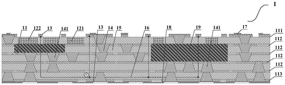
[0052] like figure 1 As shown, an airtight and high thermal conductivity LCP packaging substrate of this embodiment includes:

[0053] The n-layer patterned metal circuit layer is distributed from the surface to the bottom surface, and the n-th layer of the patterned metal circuit layer on the bottom surface is provided with a structure for soldering BGA solder balls;

[0054] n-1 insulating dielectric layers between adjacent patterned metal circuit layers;

[0055] a plurality of blind trenches of the first patterned metal circuit layer with openings facing the surface in the insulating dielectric layer between the first patterned metal circuit layer and the second patterned metal circuit layer; the blind trenches include Ordinary chip mounting blind slot and high-power chip mounting blind slot;

[0056] A metal block located in the insulating dielectric layer and connected to the bottom of the blind slot for high-power chip mounting;

[0057] A plurality of blind vias pen...

Embodiment 2

[0076] like Figure 5 As shown, based on the LCP packaging substrate described in Embodiment 1, this embodiment provides a multi-chip system-in-package structure 61, including: the LCP packaging substrate 1 described in Embodiment 1, and BGA solder balls 2 and chips 3 , metal enclosure 5 and metal cover 6;

[0077] The BGA solder balls 2 are welded to the bottom surface of the LCP package substrate 1, and serve as the external secondary cascade I / O interface of the multi-chip system-in-package structure 61;

[0078] Metal partition ribs 51 are distributed in the metal enclosure frame 5; the metal enclosure frame 5 and the metal partition ribs 51 are welded to the upper surface of the LCP package substrate 1, and the metal cover plate 6 is welded to the metal enclosure frame 5 and the metal partition ribs On 51, between the LCP package substrate 1 and the metal cover plate 6, a plurality of cavity structures 7 with airtight packaging performance and electromagnetic shielding p...


PUM


Abstract

The invention discloses an airtight high-thermal-conductivity LCP packaging substrate and a multi-chip system-in-package structure. The LCP packaging substrate comprises n graphical metal circuit layers distributed from the surface to the bottom surface, wherein the n graphical metal circuit layer on the bottom surface is provided with a structure used for welding BGA solder balls; n-1 insulating dielectric layers which are positioned between the adjacent graphical metal circuit layers; a plurality of blind grooves which are positioned in the insulating medium layer between the first graphical metal circuit layer and the second graphical metal circuit layer, wherein openings of the blind grooves face the first graphical metal circuit layer on the surface, each blind grooves comprises acommon chip mounting blind groove and a high-power chip mounting blind groove; a metal block which is positioned in the insulating dielectric layer and is connected with the bottom of the high-powerchip mounting blind groove; and a plurality of blind holes which penetrate through and are connected with the adjacent graphical metal circuit layers. The LCP package substrate can meet the system-in-package requirements of multiple chips, high airtightness requirements, high electromagnetic shielding, high thermal conductivity requirements and high reliability interconnection.

Description

technical field [0001] The invention relates to the technical field of integrated circuits and chip packaging, in particular to an airtight and high thermal conductivity LCP packaging substrate and a multi-chip system-level packaging structure for high-reliability system-level packaging for radio frequency, microwave, millimeter wave and other high-frequency applications. Background technique [0002] With the advancement of semiconductor and integrated circuit technology, the requirements for system integration have been further improved. The current electronic circuit design and manufacturing are developing towards smaller size and higher integration density. A considerable amount of work is carried out in the field of multi-chip packaging. In the advanced packaging form, multiple radio frequency (RF) chips, digital integrated circuit (IC) chips, micro-miniature chip components, etc. are assembled on the packaging substrate through SIP technology, and then integrated into a...

Claims


Application Information

Patent Timeline
Patent Type & Authority Applications(China)
IPC IPC(8): H01L23/538H01L23/367H01L23/373H01L23/498H01L23/552
CPCH01L23/49894H01L23/49838H01L23/5386H01L23/552H01L23/367H01L23/3736H01L23/49816H01L2224/48091H01L2924/00014
Inventor 戴广乾徐诺心林玉敏曾策易明生谢国平匡波卢军徐榕青向伟玮
Owner SOUTHWEST CHINA RES INST OF ELECTRONICS EQUIP
Why Eureka
Try Eureka